Intel Demos Meteor Lake CPU with On-Package LPDDR5X
Intel preps Meteor Lake processors with integrated LPDDR5X

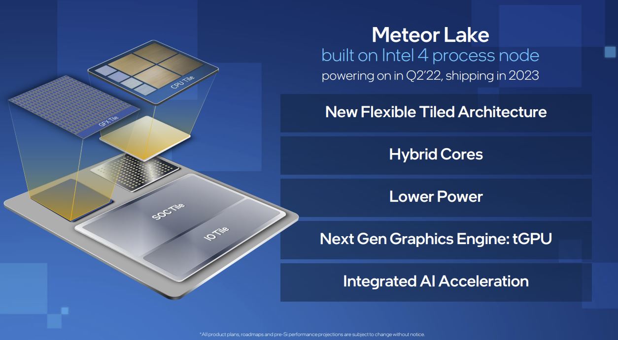
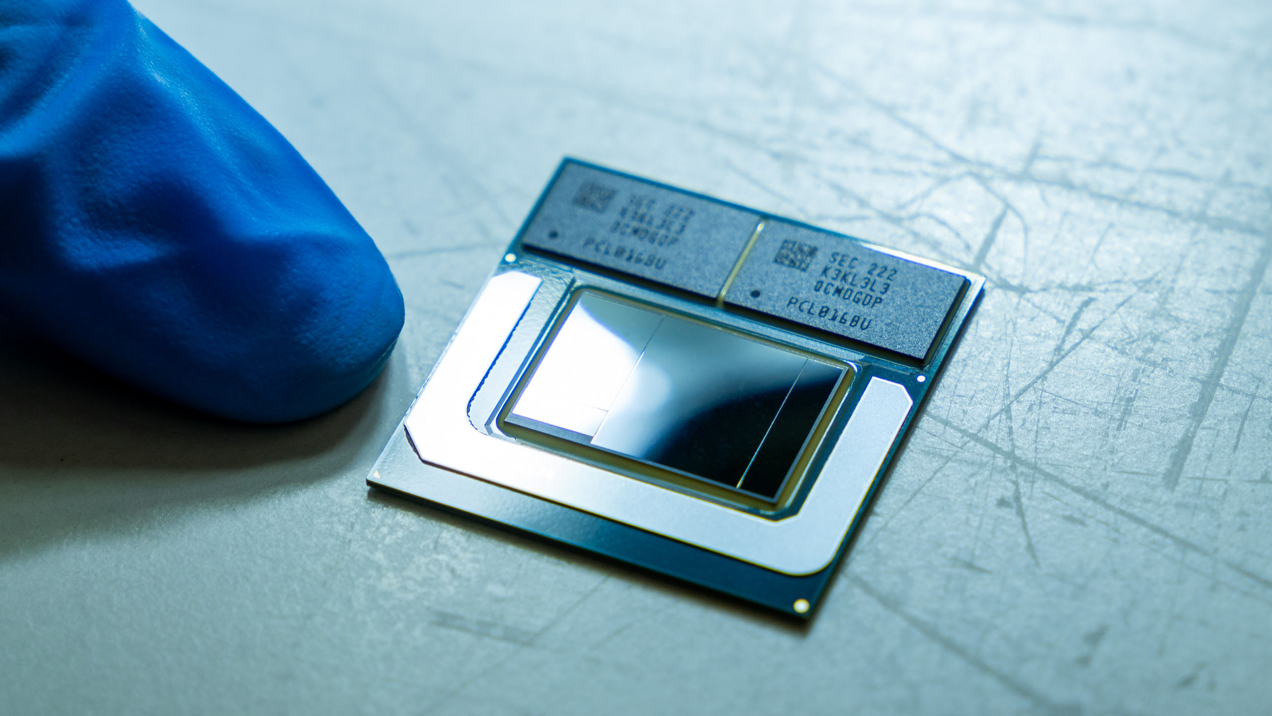
Intel on Wednesday demonstrated advancements of its sophisticated packaging technologies such as EMIB (embedded multi-die interconnect bridge) and Foveros and showed off its upcoming Meteor Lake processor with on-package LPDDR5X memory. It looks like Intel has taken a page from Apple's book as the company has been installing LPDDR memory on its M1 and M2 packages for a while now.
The product demonstrated by Intel is its quad-tile Meteor Lake CPU, which uses Foveros packaging for its chiplets and carries 16GB of Samsung's LPDDR5X-7500 memory. Actual configuration of the CPU is unknown, but 16GB of memory can provide a peak bandwidth of 120 GB/s, which is considerably higher than the peak bandwidth provided by a memory subsystem featuring DDR5-5200 or LPDDR5-6400.
Putting memory on package with the CPU brings several major advantages, including an increase in performance, a thinner system, and a reduced footprint for the platform — which allows for a larger-capacity battery. There are also disadvantages, however: if a memory chip fails, the whole system fails; platforms with everything soldered down cannot be upgraded; and cooling down both the CPU and the memory requires a more sophisticated cooling system.
Apple was the first company to use on-package LPDDR memory with a client CPU, but Intel has used package-on-package DRAM with its Atom-branded CPUs for tablets and ultra-thin laptops for years. Most recently Intel even used in-package DRAM with its first hybrid CPU called Lakefield.
What remains to be seen is whether laptop makers will bite on Intel's Meteor Lake with on-package LPDDR5X. While this simplifies manufacturing and allows them to make thinner notebooks, it also reduces their flexibility when it comes to configuration. It will also reduce the volumes of memory they procure from DRAM vendors, such as Samsung, directly, which will affect their leverage to negotiate DRAM pricing.
Get Tom's Hardware's best news and in-depth reviews, straight to your inbox.

Anton Shilov is a contributing writer at Tom’s Hardware. Over the past couple of decades, he has covered everything from CPUs and GPUs to supercomputers and from modern process technologies and latest fab tools to high-tech industry trends.
-
ezst036 ReplyAdmin said:It looks like Intel has taken a page from Apple's book as the company has been installing LPDDR memory on its M1 and M2 packages for a while now.
The product demonstrated by Intel is its quad-tile Meteor Lake CPU, which uses Foveros packaging for its chiplets and carries 16GB of Samsung's LPDDR5X-7500 memory. Actual configuration of the CPU is unknown, but 16GB of memory can provide a peak bandwidth of 120 GB/s
Looks like this sits firmly inbetween M1 and M1 Pro.
https://www.tomshardware.com/news/apple-m1-pro-max-everything-we-know
68.25 GBps200 GBps
Just a little bit above M2, which is 100Gbps. And what level is this anyways, like a level 9 cache? -
JamesJones44 If the performance and battery life are there I think OEMs like Dell and HP will bite all day long. Your lower end is doubtful, but we will see.Reply -
rluker5 I like the on package memory. Even if it only helps performance and efficiency a bit that is better than nothing.Reply
But where is this interposer with the cache that was rumored. I had my hopes up.
Also Apple was first with the on package dram, but that was with Crystalwell, an Intel product back in 2014. -
JamesJones44 The big question I have is does the iGPU have access to this memory in the same way Apple Silicon does? If it does there could be a nice boost for the iGPU in these processors. If not, it may not be as dramatic of a bump that Apple Silicon gets from it's Unified Memory structure.Reply -
jkflipflop98 Replyrluker5 said:I like the on package memory. Even if it only helps performance and efficiency a bit that is better than nothing.
But where is this interposer with the cache that was rumored. I had my hopes up.
Also Apple was first with the on package dram, but that was with Crystalwell, an Intel product back in 2014.
Wut? Exactly what advantages do you suppose putting cache on the interposer will provide? How would you even use that? The interposer is a fancy smart breadboard and nothing more. It's just wires. There's no need to shove transistors in there. -
kwohlt Reply
The advantage of 3D stacking is die space. The die doesn't have room for the rumored 128MB of L4 cache. The rumor was 3D stacked cache by placing the L4 in the active interposer, which would also allow better cooling as the compute tile would be in direct contact with the IHS, rather than being beneath the cache as X3D does.jkflipflop98 said:Wut? Exactly what advantages do you suppose putting cache on the interposer will provide? How would you even use that? The interposer is a fancy smart breadboard and nothing more. It's just wires. There's no need to shove transistors in there. -
hilive This would be ideal for appliance-type devices for which people never upgrade the RAM anyway. Examples:Reply
1. Chromebooks
2. tablets
3. ultrabooks
4. gaming consoles (Steam Deck competitors)
And the idea that the integrated RAM will make heat problems significantly worse is strange. First off, this isn't going to be used on workbooks with 32 or 64 GB RAM. It is going to be used for consumer and prosumer devices like the Dell XPS 13. Even if it did, the node shrink - going from 10nm for Raptor Lake to 7nm for Meteor Lake - would more than overcompensate for it anyway. -
Lucky_SLS They could have gone with 24gb Memory considering that igpu would use from the same Memory pool.Reply
This would be an interesting AMD Z1 extreme competitor. -
jkflipflop98 Replykwohlt said:The advantage of 3D stacking is die space. The die doesn't have room for the rumored 128MB of L4 cache. The rumor was 3D stacked cache by placing the L4 in the active interposer, which would also allow better cooling as the compute tile would be in direct contact with the IHS, rather than being beneath the cache as X3D does.
Your OP didn't say anything about die stacking. You said "where is this interposer with the cache that was rumored." Foveros doesn't need cache itself. You add cache by stacking it on top. There's no need for it to be IN the breadboard. -
abufrejoval Reply
I guess you refer to the 64/128MB of EDRAM for GPU use and this is what I had to immediately think of, too. I have several systems with EDRAM and bigger iGPUs with 48EUs, but they yield very poor performance increases and feel more like a 24->32EU upgrade than the doubling they should have delivered. And then Xe with 96EUs does offer a linear 4x upgrade over the prevous 24EU iGPUs without any of the EDRAM overhead!rluker5 said:I like the on package memory. Even if it only helps performance and efficiency a bit that is better than nothing.
But where is this interposer with the cache that was rumored. I had my hopes up.
Also Apple was first with the on package dram, but that was with Crystalwell, an Intel product back in 2014.
In terms of Apple pushing and Intel implementing I'd say you'd call that "co-creation" and outsiders might never know who led with the idea.
The current Apple design eliminates all external DRAM interfaces from the die carrier and that is obviously a big save in terms of power and cost, but means a complete loss of RAM expansion.
So that for me is the biggest question and so far without any indication which way Intel would want to go here: do they cut external RAM or do they allow external expansion?
And how would that be implemented and work?
I own an Alder lake laptop that has 8GB of soldered DRAM and a SO-DIMM slot that was originally filled with a matching 8GB DDR4 SO-DIMM for a fully matched dual-channel setup. But since I often need to operate with VMs and RAM is so extraordinarily cheap these days (unless you buy from Apple), I replaced the 8GB stick with a 32GB variant, fully aware that this would reduce the upper 24GB or RAM to single channel operations and bandwidth.
My rationale is that it's still way faster then paging and that the most bandiwidth critical part, the iGPU frame buffer would be taken from the bottom physical RAM which would remain dual-channel.
But how would this now work out with a chip like this? Dual channel operations seem pretty much out of reach, when latencies and general characteristics are as far out of step as they would be here. Running two distinct single-channel memory pools doesn't seem very attractive either, which seems to provide a strong hint, that this type of chip would cut memory expansion entirely like Apple's Mx designs.
Except that those have this trick up their sleves, where they use multiples of the base chip including each with its DRAM package to combine into x2 and x4 designs, that then are effectively doubling or quadrupling the memory channels and bandwidths accordingly.
There is no obvious way this could happen with the Intel variant, judging from the provided picture. Yet without such a scaling escape hatch, their approach no longer looks terribly attractive.
I do think that having both on-die (or on-substrate) extra DRAM together with more traditional external DRAM is attractive, but only if that on-die DRAM is wide and fast enough to carry all iGPU burdens with ease.
But that would likely require a completely distinct memory controller with another set of channels and therefore a chip re-design that's far from minor... and therefore hard to imagine, even if Intel has far less qualms about designing fully distinct die variants than AMD.
In other words: this article unforunately creates more questions than I feel it answers.
