PSU Repair: A Case Study
When your PSU won't start, most enthusiasts don't go beyond a paperclip or multimeter check. Today, we'll do a comprehensive repair of Antec's old SL300.
Get Tom's Hardware's best news and in-depth reviews, straight to your inbox.
You are now subscribed
Your newsletter sign-up was successful
Auxiliary Output Replacement?
Based on the weak and jagged main output ramp on the previous page and my earlier hypothesis that the main converter IC is not receiving sufficient power to operate normally, I would say almost certainly yes. The nice thing about knowing how the circuit works and having an oscilloscope is that I can hook it up and see how badly.


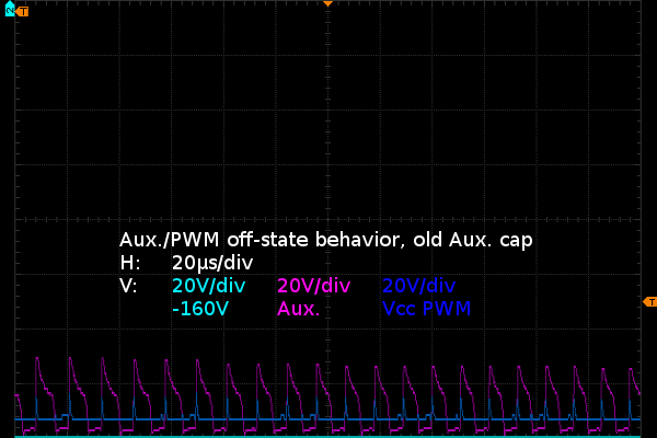
The first slide shows the bottom capacitor voltage, auxiliary output voltage and PWM controller supply voltage while the main outputs are off. Something looks very wrong here. I was expecting to find out what the nominal voltage on the auxiliary supply was, but its waveform peaks at -132V and does not appear to be holding any voltage at all, dropping to about -156V half-way between pulses. This is so different from what I was expecting to see that I had doubts about somehow soldering my probe wire to the wrong trace--the long, relatively fat, unmistakable one that links the auxiliary output to the PWM section. On the PWM's side, the fast edges from the auxiliary supply ripples are causing glitches to pass through. However, the output is otherwise holding steady at about 8V, which is consistent with the 3844B's under-voltage lock-out, so the PWM's bypass capacitor might still be good. Perhaps one of the other operating states will shed some more light.
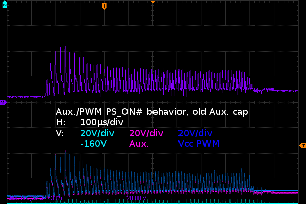
The second slide shows what happens to the auxiliary and PWM supply nodes when the main outputs are trying to turn on. The math channel shows the voltage across the PWM's supply bypass capacitor. There is nearly 20VPP of noise on the controller's supply and the DC value is barely 10V with some dips below its under-voltage threshold. Not many chips will operate well when their supply has nearly twice as much noise as it does DC, on top of input voltage being barely above the minimum operating voltage. The W12NK80 MOSFET used in this power supply needs at least 8V to switch 6A, but the PWM controller needs to have a supply a few volts higher than that to offset its own gate drive's voltage drop and the voltage drop across external gate drive components, meaning 10V is nowhere near enough for reliable operation.
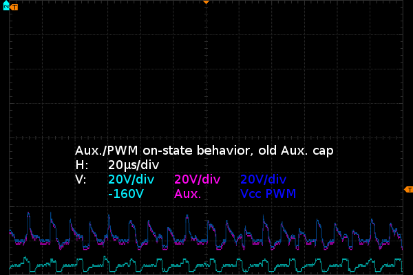
Article continues belowThe final slide shows what happens when the PWM manages to turn on. I forgot to enable the math channel on this one, but if you use a little imagination to extrapolate the voltage between the bottom capacitor voltage and aux/PWM supply voltage, you can see the controller IC's input voltage is still quite messy. If you have trouble imagining this, look at areas where the cyan line and the two others move in opposite directions. Those would be spikes, many large ones at that. With finer time resolution, we can see that the PWM supply voltage is tracking AUX voltage almost perfectly, indicating that the photocoupler has no trouble driving its pass transistor into saturation to feed the main switcher, so we can dismiss the on/off control photocoupler and its pass transistor as potential concerns. We can also see fairly well that the auxiliary voltage is about 20V above the bottom cap voltage on average.
The auxiliary cap definitively needs to be replaced, and given the way the PWM bypass capacitor tracks it, there is a high probability it needs replacement too. If the PWM's bypass capacitor still had even 1µF of its nominal 22µF left, I would expect to see that charge decay over a few microseconds between top-offs by auxiliary peaks instead of momentary glitches.
If this was a normal repair job, I would replace both on the same soldering iron run and ask questions later. But since I am taking a case study approach, I am fixing problems singularly so that I can observe, analyze and comment on causes and effects, one variable at a time.
Get Tom's Hardware's best news and in-depth reviews, straight to your inbox.
Current page: Auxiliary Output Replacement?
Prev Page 5VSB Capacitor Replacement Next Page Auxiliary Output Capacitor Replacement-
Nuckles_56 An interesting read, it was interesting following the process you used to troubleshoot the problemReply -
Crashman I used to do this for a living :)Reply
Don't tell my boss, I've managed to convince him that I'm only an expert at running benchmarks and writing about the results :) -
epsiloneri Disclaimers won't help. The people who will likely hurt themselves trying this are the same who lack the reading comprehension and self awareness to understand those disclaimers are directed at them. I admire you courage in publishing this.Reply
-
beetlejuicegr the truth is the paper clip and multimeter is all i can go in to psus. after all i haven't studied electricity or circuits or whatever.Reply
However i do hate to throw stuff earlier than it should, like you. -
C12Friedman I like this article and I fully agree with the conclusion. I've repaired a few PSU's but, for the most part I scavenge them anymore since I can't put them in a new system (nor would I want to) IMO they aren't really worth anything other than for on a test bench.Reply -
Mr A Daniel, I know next to nothing about electronics, and yet I could not stop reading this article. Fascinating! Thanks very much!Reply -
Urzu1000 This was a great article! It was informative, as well as interesting. Personally, I've only had one PSU fail on me so far. My brother-in-law's self-built computer had a really low-end Thermaltake PSU. 800W Bronze, and oh man, did that thing go out in a blaze of glory. Very loud popping, and smoke, and funny smells. When I ripped it out of the computer, there were burns inside the case. Miraculously, the other components remained unharmed, so I slapped in a new PSU (750W Gold Seasonic) and fired it up.Reply
Still working good, but I get black soot on my hands every time I open up that case. It's a black case, so it's hard to clean it off properly. -
Interesting article. I would have simply replaced the entire unit. You saw how to fix the failure, but how many units were damaged that you didn't see? A ticking time bomb that will eventually send some spike to your much more valuable hardware than a 10 year old PSU. Wasteful, yes. I get it. I don't like to waste either. And if it's on marginal hardware, fine. But on primary systems I'm not willing to take the risk. I'd rather throw away a 200$ part that has a 0.05$ repair solution, than risk frying 800$+ hardware.Reply
-
kalmquist "Antec's manufacturer (Channelwell in this case) got the live and neutral wires backwards, which means that in the “off” position, the neutral line gets opened and everything on the primary side becomes live instead of neutral."Reply
That's really bad--I doubt it is even legal to sell a power supply wired like that. I've never bought a CWT (Channelwell) power supply, and based on this I wouldn't buy one, except perhaps for a high end model where you might gamble that the company would exercise a bit more care.