ATI Enters The X1000 Promised Land
To The Core
There has been a lot of speculation about the makeup of this new architecture but we can finally shed some light on the truth. You no longer have to go see what Fudo has posted about R520 on the Inquirer. That being said, unlike the positioning of extra math units in the pixel pipeline, as was the case for the 7800 GTX, ATI has altered almost every segment of the architecture.
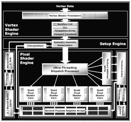
A diagram of the X1800 GPU core.
First, they changed how the data stream is processed. The flow is similar but broken up and compartmentalized to efficiently utilize all of the ALUs of the pixel shaders. They even redesigned how the shaders work. Like we said, they altered how the work gets done and ATI took the threaded approach to problem solving.
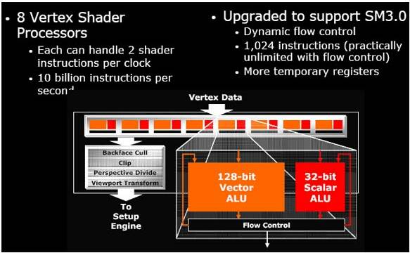
The first step in the process should be familiar to all; the data visits the 8 Vertex Shaders. ATI refers to their approach as "SM 3.0 done right." They even told us that the Shader Model 3.0 X1000 family has passed Microsoft's Display Compatibility Test (DCT).
The vertex shaders can handle two vertex instructions per clock or roughly 10 billion instructions per second. This is possible because each of the shaders has two ALUs; one 128-bit vector ALU and one 32-bit scalar ALU. This allows for "full-time" 32-bit floating point precision. Included in each shader is a flow control unit to keep the process moving.
Once the back-face culling, clipping, perspective divide (transform to clip space), viewpoint transform and other geometry operations are done, the next stop is to the setup engine which includes a geometry rasterization unit. From there the pixel data goes to a new "Ultra-Threading" dispatch processor. This processor breaks the shader data into as many as 512 parallel threads. Here is where ATI gets a huge boost to performance, through the optimization of the pixel shaders as well as through the new design of the memory architecture (which we will go through later).
Get Tom's Hardware's best news and in-depth reviews, straight to your inbox.

