AMD FirePro W9100 Review: Hawaii Puts On Its Suit And Tie
AMD's Hawaii GPU makes its appearance in the workstation space as FirePro W9100. Does this $4000 card have what it takes to displace Nvidia's Quadro K6000, or is it a more conservative performer? We throw an exhaustive benchmark suite at it to find out.
Get Tom's Hardware's best news and in-depth reviews, straight to your inbox.
You are now subscribed
Your newsletter sign-up was successful
The Differences Between Hawaii And Tahiti GPUs
While Hawaii's 438 mm² die is still smaller than the GK110 on Nvidia's Quadro K6000, it's the largest GPU AMD has ever manufactured. The legendary R600 was a "mere" 420 mm².
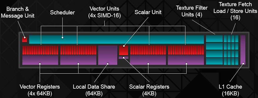
In most respects, the implementation of AMD's Graphics Core Next architecture on Hawaii is almost identical to the FirePro W9000’s Tahiti GPU. Specifically, the Compute Unit building block is the same. All 64 IEEE-754-2008-conformant shaders consist of four vector and sixteen texture fetch load/store units.
There are, of course, improvements over the Tahiti GPU on AMD's FirePro W9000, such as device flat addressing to support standard calling conventions, precision improvements to the native LOG and EXP operations, and optimizations to the Masked Quad Sum of Absolute Difference (MQSAD) function, speeding up algorithms for motion estimation.
Article continues belowAnd with the introduction of DirectX 11.2, programmable LOD clamping and the ability to tell a shader if a surface is resident were added. Both are tier-two features associated with tiled resources.
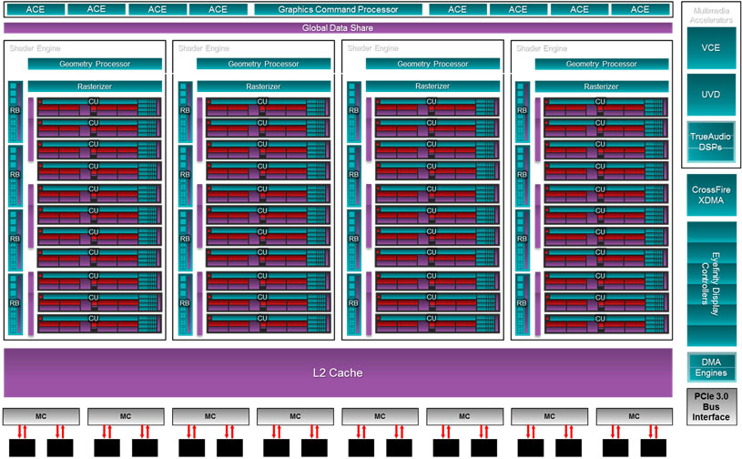
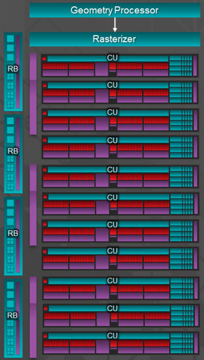
The main departure from the W9000's GPU is the arrangement of Compute Units. Whereas Tahiti employs 32 CUs, totaling 2048 shaders and 128 texture units, Hawaii wields 44 CUs organized into four of what AMD calls Shader Engines. The math adds up to 2816 aggregate shaders and 176 texture units.
The new GPU employs eight revamped Asynchronous Compute Engines, responsible for scheduling real-time and background tasks to the CUs. The W9000 has only two. Each ACE manages up to eight queues, totaling 64, and has access to L2 cache and shared memory.
It makes a lot of sense to dedicate more resources to the arbitration of GPU resources between computation and graphics; this improves overall efficiency.
Get Tom's Hardware's best news and in-depth reviews, straight to your inbox.
The W9000’s front-end fed vertex data to the shaders through a pair of geometry processors. Given its quad-Shader Engine layout, the FirePro W9100 doubles that number, facilitating four primitives per clock cycle instead of two. There’s also more inter-stage storage between the front- and back-end to hide latencies and realize as much of that peak primitive throughput as possible.
In addition to a dedicated geometry engine (and 11 CUs), Shader Engines also have their own rasterizer and four render back-ends capable of 16 pixels per clock. That’s 64 pixels per clock across the GPU—twice what the W9000’s GPU could do. The W9100’s Hawaii chip enables up to 256 depth and stencil operations per cycle, again doubling Tahiti’s 128.
On a graphics card designed for high resolutions, a big pixel fill rate comes in handy, and, according to AMD, in many cases, this shifts the chip’s performance bottleneck from fill to memory bandwidth.
The shared L2 read/write cache grows from 768 KB in Tahiti to 1 MB, divided into 16 64 KB partitions. This 33% increase yields a corresponding bandwidth increase between the L1 and L2 structures of 33% as well, topping out at 1 TB/s.
It makes sense, then, that increasing geometry throughput, adding 768 shaders, and doubling the back-end’s peak pixel fill would put additional demands on Hawaii’s memory subsystem. AMD addresses this with a redesigned controller.
The new GPU features a 512-bit aggregate interface that the company says occupies about 20% less area than Tahiti’s 384-bit design and enables 50% more bandwidth per mm².
How is this possible? It actually costs die space to support very fast data rates. So, hitting 6 Gb/s at higher voltage made Tahiti less efficient than Hawaii’s bus, which targets lower frequencies at lower voltage, and can consequently be smaller. Operating at 5 Gb/s in the case of the FirePro W9100, the 512-bit bus pushes up to 320 GB/s. In comparison, Tahiti maxed out at 288 GB/s.
Current page: The Differences Between Hawaii And Tahiti GPUs
Prev Page Hawaii Goes Professional Next Page FirePro W9100: Dimensions, Weight, And Features
Igor Wallossek wrote a wide variety of hardware articles for Tom's Hardware, with a strong focus on technical analysis and in-depth reviews. His contributions have spanned a broad spectrum of PC components, including GPUs, CPUs, workstations, and PC builds. His insightful articles provide readers with detailed knowledge to make informed decisions in the ever-evolving tech landscape
-
CodeMatias "Nvidia’s sub-par OpenCL implementation"Reply
Right... that's why in real-world functions (rather than "perfect" functions used in benchmarks) the nvidia cards are on par with or even better than the AMD ones... What the author fails to understand is that AMD is the one with sub-par implementation of OpenCL, since half the language is missing in their drivers (and why groups like Blender and Luxrender have to drop support for most things to have the kernel compile properly). Sure the half of the language that is there is fast, but it's like driving a three wheeled ferrari! -
Kekoh I'll be honest, I don't know anything about workstation graphics. I read this purely for knowledge. That being said, I can't help but pick up on the AMD bias in this article.Reply -
sha7bot Amazing card, but I disagree with your thoughts on the price. Anyone in this segment will drop another 1k for NVIDIA's consistent reliability.Reply
If AMD wants to take more market share from NVIDIA, it needs to lower the pricing to appeal to a larger audience and when the IT team is convincing purchasing, 1k isn't much in the long run. They need to drop there price so it's hard to pass up. -
Shankovich A great card to be honest. I had one sent to me by AMD and I've been tinkering with it today to run CFD software, along with some CFD code. It really sped things up a lot! Though the drivers need work however.Reply
I only think AMD really needs to beef up that cooler. A triple slot perhaps? (make the blower two slots). That thermal ceiling is holding a lot back. -
Jarmen Kell with this performance the W9100 really has a great value, some tests feel's like driving a fast four wheeled fully opencl accelerated Mclaren F1,nice review.Reply -
mapesdhs The picture is incomplete though without comparing to how the Quadro wouldReply
perform when using its native CUDA for accelerating relevant tasks vs. the
FirePro using its OpenCL, eg. After Effects. Testing everything using OpenCL
is bound to show the FirePro in a more positive light. Indeed, based on the
raw specs, the W9100 ought to be a lot quicker than it is for some of the tests
(Igor, ask Chris about the AE CUDA test a friend of mine is preparing).
Having said that, the large VRAM should make quite a difference for medical/GIS
and defense imaging, but then we come back to driver reliability which is a huge
issue for such markets (sha7bot is spot on in that regard).
Ian.
-
wekilledkenny WTH is "Drawed Objects"? Even a rudimentary spell-check can catch this.Reply
For an English irregular verb "to draw" the perfect tense is "drawn" (and the past is "drew").
For an organization claiming to be professional enough to do a review of a professional grade GPU, simple things like that can take away a lot of credibility. -
Marcelo Viana ReplyThe picture is incomplete though without comparing to how the Quadro would
perform when using its native CUDA for accelerating relevant tasks vs. the
FirePro using its OpenCL, eg. After Effects. Testing everything using OpenCL
is bound to show the FirePro in a more positive light. Indeed, based on the
raw specs, the W9100 ought to be a lot quicker than it is for some of the tests
(Igor, ask Chris about the AE CUDA test a friend of mine is preparing).
Having said that, the large VRAM should make quite a difference for medical/GIS
and defense imaging, but then we come back to driver reliability which is a huge
issue for such markets (sha7bot is spot on in that regard).
Ian.
Then put a box with 8 k6000(8 is the total of cards that the "Nvidia maximum" alow) against 4 w9100(4 is the total of cards that amd said that should put in one system).
Do you think it is fair? From the point of view of a renderfarm owner perhaps, because he dont look at a card but at a solution. Also dont forget that he have to deal with the price(8 $5K($40,000) against 4 $4K($16,000)) maybe he find that the cheaper solution isn't the faster one but maybe faster enough.
But here they put a card against a card. And for me the only way is openCL because it is open. You cant benchmark over a proprietary maner. You must use a tool that both contenders can read.
And yes NVidia dont give a shit to openCL, and i understand why, but i dont think it's wise. time will tell. -
mapesdhs Marcelo Viana writes:Reply
> Then put a box with 8 k6000(8 is the total of cards that the "Nvidia maximum" alow) ...
You'd need to use a PCIe splitter to do that. Some people do this for sure, eg. the guy
at the top of the Arion table is using seven Titans, but PCIe splitters are expensive, though
they do offer excellent scalability, in theory up to as many as 56 GPUs per system using
8-way splitters on a 7-slot mbd such as an Asrock X79 Extreme11 or relevant server board.
> Do you think it is fair? ...
Different people would have varying opinions. Some might say the comparison should be based on a fixed
cost basis, others on power consumption or TCO, others on the number of cards, others might say 1 vs. 1
of the best from each vendor. Since uses vary, an array of comparisons can be useful. I value all data points.
Your phrasing suggests I would like to see a test that artifically makes the NVIDIA card look better, which is
nonsense. Rather, atm, there is a glaring lack of real data about how well the same NVIDIA card can run a
particular app which supports both OpenCL and CUDA; if the CUDA performance from such a card is not
sufficiently better than the OpenCL performance for running the same task, then cost/power differences
or other issues vs. AMD cards could mean an AMD solution is more favourable, but without the data one
cannot know for sure. Your preferred scope is narrow to the point of useless in making a proper
purchasing decision.
> But here they put a card against a card. And for me the only way is openCL because it is open. ...
That's ludicrous. Nobody with an NVIDIA card running After Effects would use OpenCL for GPU acceleration.
> ... You must use a tool that both contenders can read.
Wrong. What matters are the apps people are running. Some of them only use OpenCL, in which case
sure, run OpenCL tests on both cards, I have no problem with that. But where an NVIDIA card can offer
CUDA to a user for an application then that comparison should be included aswell. To not do so is highly
misleading.
Otherwise, what you're saying is that if you were running AE with a bunch of NVIDIA cards then
you'd try to force them to employ OpenCL, a notion I don't believe for a microsecond.
Now for the apps covered here, I don't know which of them (if any) can make use of CUDA
(my research has been mainly with AE so far), but if any of them can, then CUDA-based
results for the relevant NVIDIA cards should be included, otherwise the results are not a
true picture of available performance to the user.
Atm I'm running my own tests with a K5000, two 6000s, 4000, 2000 and various gamer cards,
exploring CPU/RAM bottlenecks.
Btw, renderfarms are still generally CPU-based, because GPUs have a long way to go before they can
cope with the memory demands of complex scene renders for motion pictures. A friend at SPI told me one
frame can involve as much as 500GB of data, which is fed across their renderfarm via a 10GB/sec SAN. In
this regard, GPU acceleration of rendering is more applicable to small scale work with lesser data/RAM
demands, not for large productions (latency in GPU clusters is a major issue for rendering). The one
exception to this might be to use a shared memory system such as an SGI UV 2 in which latency is no
longer a factor even with a lot of GPUs installed, and at the same time one gains from high CPU/RAM
availability, assuming the available OS platform is suitable (though such systems are expensive).
Ian.
-
Marcelo Viana good answer mapesdhs, and i agree with almost everything you posted, but yet i think you didn't got what i meant to explain in my replay.Reply
You saying that the point of view must be based on software people use. Of course i'll make my decision to or not to buy a card on the software i use. I totally agree with you on that (if it's what you mean), but benchmark is another, completely different thing.
"You must use a tool that both contenders can read." isn't a wrong statement. My thing is render so i'll keep on that: I-Ray is a software to render on GPU, but use only cuda (unable to do this benchmark) VRay-RT is another software that can render on cuda and on openCL (still unable to do this benchmark unless you use openCL only).
If you gonna benchmark not the cards, but this two software ok, you can use a Nvidia card and benchmark this two software on cuda, and even that the card can read cuda and openCL, you must not use openCL, because one of the contenders(I-Ray) cannot read openCL.
In other way if you decide to use the software VRay-RT you can use a Nvidia card and benchmark using cuda and openCL to see what is better, but you can't use AMD card on that.
Perhaps, outside of benchmark world of course i can use Nvidia card, AMD card, I-Ray, Vray-RT, whatever i want. But on this review they do benchmark to compare two cards for god's sake.
Benchmark means: a software common to contenders to judge this contenders.
I hope you understand the meaning of my post this time.
In time: i understood your point of view and i agree with that, except benchmark.


