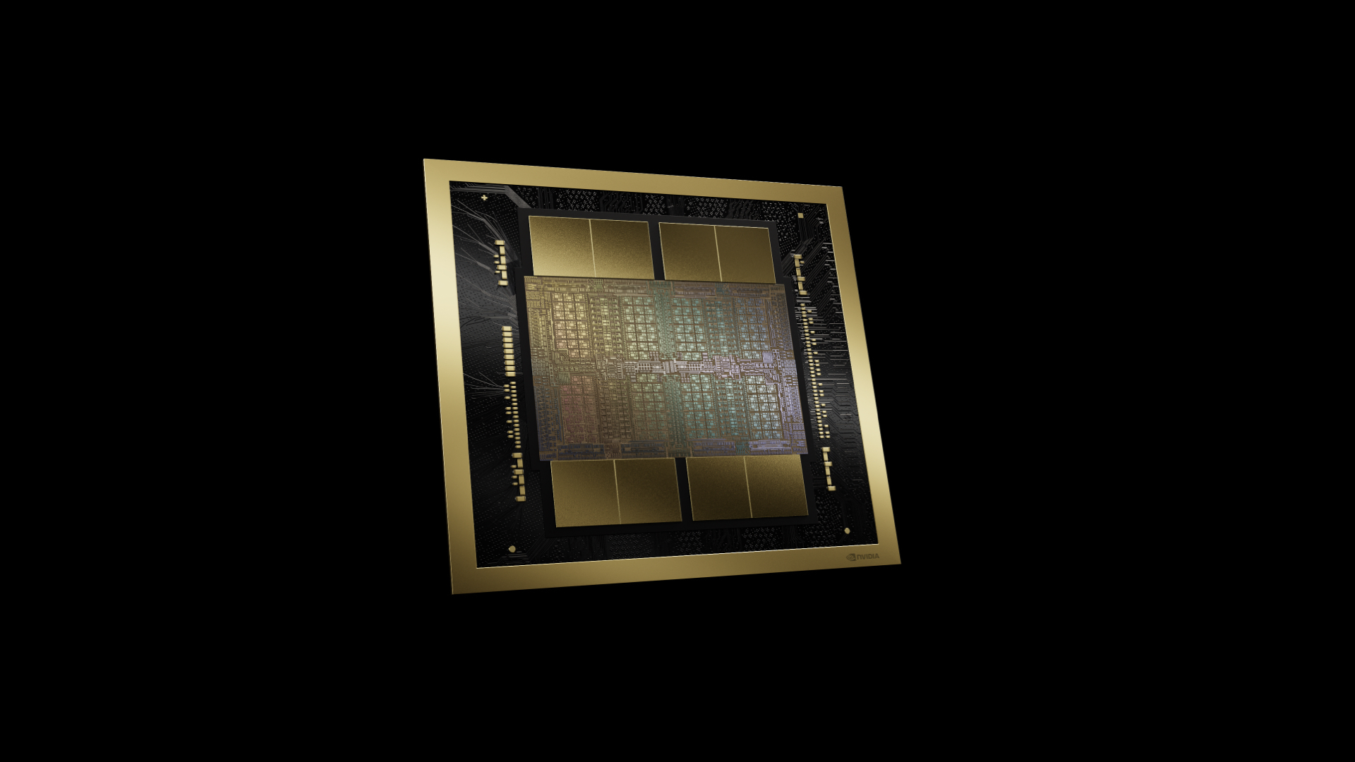
Nvidia publishes first Blackwell B200 MLPerf results: Up to 4X faster than its H100 predecessor, when using FP4
There are quite a few caveats and qualifications to that figure.

Nvidia has published the first MLPerf 4.1 results of its Blackwell B200 processor. The results reveal that a Blackwell GPU offers up to four times the performance of its H100 predecessor based on the Hopper architecture, highlighting Nvidia's position as the leader in AI hardware. There are some caveats and disclaimers that we need to point out, however.
Based on Nvidia's results, a Blackwell-based B200 GPU delivers 10,755 tokens/second on a single GPU in a server inference test and 11,264 tokens/second in an offline reference test. A quick look at the publicly available MLPerf Llama 2 70B benchmark results reveals that a 4-way Hopper H100-based machine delivers similar results, lending credence to Nvidia's claim that a single Blackwell processor is about 3.7X– 4X faster than a single Hopper H100 GPU. But we need to dissect the numbers to better understand them.
| Row 0 - Cell 0 | # of GPUs | Offline | Server | per GPU Offline | per GPU Server |
| Nvidia B200 180GB HBM3E | 1 | 11264 | 10755 | 11264 | 10755 |
| Nvidia H100 80GB HBM3 | 4 | 10700 | 9522 | 2675 | 2381 |
| Nvidia H200 141GB HBM3E | 1 | 4488 | 4202 | 4488 | 4202 |
| Nvidia H200 141GB HBM3E | 8 | 32124 | 29739 | 4016 | 3717 |
First, Nvidia's Blackwell processor used FP4 precision as its fifth generation Tensor Cores support that format, whereas Hopper-based H100 only supports and uses FP8. These differing formats are allowed by MLPerf guidelines, but FP4 performance in Blackwell doubles its FP8 throughput, so that's the first important item of note.
Next, Nvidia is somewhat disingenuous in using a single B200 versus four H100 GPUs. Scaling is never perfect, so a single-GPU tends to be something of a best-case scenario for per-GPU performance. There are no single-GPU H100 results listed for MLPerf 4.1, and only a single B200 result, so it becomes even more apples and oranges. A single H200 achieved 4,488 tokens/s, however, which means B200 is only 2.5X faster for that particular comparison.
Memory capacity and bandwidth are also critical factors, and there are big generational differences. The tested B200 GPU carries 180GB of HBM3E memory, H100 SXM has 80GB of HBM (up to 96GB in some configurations), and H200 has 96GB of HBM3 and up to 144GB of HBM3E. One result for single H200 with 96GB HBM3 only achieves 3,114 tokens/s in offline mode.
So, there are potential differences in number format, GPU count, and memory capacity and configuration that play into the "up to 4X" figure. Many of those differences are simply due to Blackwell B200 being a new chip with a newer architecture, and all of these things play into its ultimate performance.
Getting back to Nvidia's H200 with 141GB of HBM3E memory, it also performed exceptionally well not only in the generative AI benchmark featuring the Llama 2 70B large language model, but also in every single test within the datacenter category. For obvious reasons, it got significantly faster than H100 in tests that take advantage of GPU memory capacity.
For now, Nvidia has only shared performance of its B200 in the MLPerf 4.1 generative AI benchmark on Llama 2 70B model. Whether that's because it's still working on tuning or other factors we can't say, but MLPerf 4.1 has nine core disciplines and for now we can only guess how the Blackwell B200 will handle the other tests.
Get Tom's Hardware's best news and in-depth reviews, straight to your inbox.

Anton Shilov is a contributing writer at Tom’s Hardware. Over the past couple of decades, he has covered everything from CPUs and GPUs to supercomputers and from modern process technologies and latest fab tools to high-tech industry trends.
-
JRStern Very good!Reply
There was some release a few weeks ago where NVIdia was claiming more like 30x faster for the overall calculation - based on FP4! That's if you could convert all your FP8, FP16, and FP32 to FP4. Which you can't. -
Pierce2623 News Flash!!! Two chips at fp4 four times as fast as one chip at fp8!!! (Think to himself “isn’t that EXACTLY the same amount of processing power per chip?”)Reply -
YSCCC Ok, good gen on gen performance leap in theory would be attained, but can we have something budget and good performing in consumer market now?Reply -
renz496 Reply
Already have lots of them in the market. For nvidia anything below $1500 is "budget" card.YSCCC said:Ok, good gen on gen performance leap in theory would be attained, but can we have something budget and good performing in consumer market now? -
YSCCC Reply
Lol that's their definition of budget, I mean (sarcasm mode on) when will they dare separate the high margin coporate hype market vs the more civilian friending gaming offeringsrenz496 said:Already have lots of them in the market. For nvidia anything below $1500 is "budget" card. -
Kamen Rider Blade Reply
Never Again!YSCCC said:Lol that's their definition of budget, I mean (sarcasm mode on) when will they dare separate the high margin coporate hype market vs the more civilian friending gaming offerings
They know Enterprise pays more, ALOT more.
We Gamers get the left-overs / scraps. -
GenericUsername109 Nvidia is a hot business now, chasing profit margins, revenue and earnings. I bet a wafer of these datacenter chips is way more profitable than anything retail buyers can afford. They have a huge order backlog on these, too. No rush to waste precious TSMC capacity on some low margin "hobby" stuff, when they can turn it to gold and print money.Reply