Nvidia's Blackwell B100 GPU to Hit the Market with 3nm Tech in 2024: Report

Nvidia Hopper H100 die shot
(Image credit: Nvidia)

Nvidia is set to adopt TSMC's 3nm-class process technology next year, a report by DigiTimes reads. The company is expected to produce its codenamed GB100 compute graphics processor using the technology. However, it is likely that the company will produce all Blackwell GPUs using the same fabrication technology.

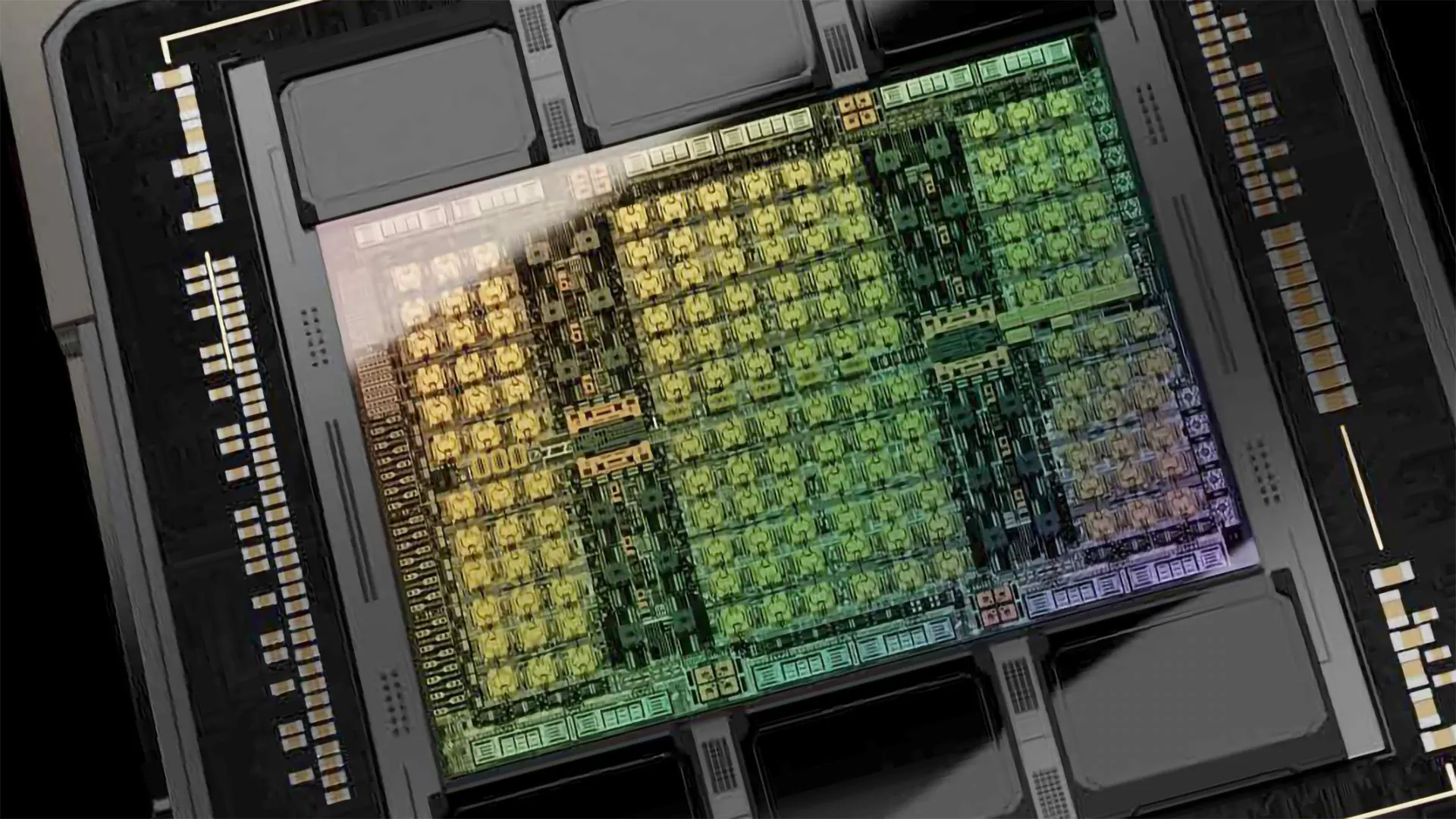
The report claims that Nvidia's GB100 is projected to be launched in 2024, which will align with Nvidia's typical two-year cadence of launching new GPU architectures. The B100 will likely be Nvidia's next-generation compute GPU product for artificial intelligence (AI) and high-performance computing (HPC) applications. Meanwhile, the latest rumors suggest that the GB100 product will use a multi-chiplet design to increase performance tangibly compared to the GH100 product based on the Hopper architecture. 

It remains to be seen which of TSMC's 3nm-class process technology will be adopted by Nvidia. TSMC has numerous 3nm nodes, including performance-enhanced N3P and HPC-oriented N3X. Nvidia has used customized fabrication technologies for its Ada Lovelace, Hopper, and Ampere GPUs, so it is possible that the company will use a custom node with its Blackwell graphics processors as well. 

Nvidia will, of course, not be alone with the adoption of TSMC's N3 technology next year: AMD, Intel, MediaTek, and Qualcomm are all set to adopt one of the foundry's 3nm-class nodes in 2024 – 2025. In fact, MediaTek has already taped out its first N3E design with TSMC. 

At present, only Apple uses TSMC's N3B (1st generation N3) technology to make its A17 Pro system-on-chip for smartphones. The technology is expected to be adopted for other SoCs, including M3, M3 Pro, M3 Max, and M3 Ultra for Mac personal computers.

Anton Shilov
Contributing Writer

Anton Shilov is a contributing writer at Tom’s Hardware. Over the past couple of decades, he has covered everything from CPUs and GPUs to supercomputers and from modern process technologies and latest fab tools to high-tech industry trends.

  • I'm somewhat embarassed that i don't fully understand this, but i'll ask anyway: is this Blackwell B100 codename only about AI GPUs, intented for enterprises, or will it also include the new RTX 50 series? Because, if memory serves, we should be expecting GeForce 50** at 2025. Can somebody please explain?
    Reply
  • kraylbak said:
    i'll ask anyway: is this Blackwell B100 codename only about AI GPUs, intented for enterprises, or will it also include the new RTX 50 series? Because, if memory serves, we should be expecting GeForce 50** at 2025. Can somebody please explain?

    Yes you are correct, these are only for the AI and HPC segment. The consumer (gaming) parts will fall under the "GB200" series and not the GB100 series, but these are just internal codenames for now. Most likely Nvidia will adopt the RTX 50-series nomenclature.

    Like mentioned, the Blackwell "GB100" series are for the AI, HPC and data center market. The lineup includes the GB100 and GB102 SKUs based on the same architecture, and internally Nvidia has labelled them as the "Classic GPUs" for now (taken from an internal source code dump file).

    NVIDIA is also working on gaming SKUs under the same Blackwell GPU architecture. A previous leak suggested that NVIDIA will have at least six SKUs in the GeForce RTX 50 gaming lineup.

    However, there's one change. The lineup would include GB202 silicon as the flagship, followed by GB203, GB205, GB206, and GB207. This lineup is still subject to change though, but more or less confirmed to be final.
    Blackwell GB202 (Top Ultra Enthusiast)
    Blackwell GB203 (Extreme/Enthusiast)
    Blackwell GB205 (High-End)
    Blackwell GB206 (Mainstream)
    Blackwell GB207 (Entry-Level)Specs speculation:

    GB202: 512bit GDDR6X/7
    GB203: 384bit GDDR6X/7
    GB205: 192bit GDDR7
    GB206: 128bit GDDR7
    GB207: 96bit GDDR7
    Reply
  • Metal Messiah. said:
    Yes you are correct, these are only for the AI and HPC segment. The consumer (gaming) parts will fall under the "GB200" series and not the GB100 series, but these are just internal codenames for now. Most likely Nvidia will adopt the RTX 50-series nomenclature.

    Like mentioned, the Blackwell "GB100" series are for the AI, HPC and data center market. The lineup includes the GB100 and GB102 SKUs based on the same architecture, and internally Nvidia has labelled them as the "Classic GPUs" for now (taken from an internal source code dump file).

    NVIDIA is also working on gaming SKUs under the same Blackwell GPU architecture. A previous leak suggested that NVIDIA will have at least six SKUs in the GeForce RTX 50 gaming lineup.

    However, there's one change. The lineup would include GB202 silicon as the flagship, followed by GB203, GB205, GB206, and GB207. This lineup is still subject to change though, but more or less confirmed to be final.
    Blackwell GB202 (Top Ultra Enthusiast)
    Blackwell GB203 (Extreme/Enthusiast)
    Blackwell GB205 (High-End)
    Blackwell GB206 (Mainstream)
    Blackwell GB207 (Entry-Level)Specs speculation:

    GB202: 512bit GDDR6X/7
    GB203: 384bit GDDR6X/7
    GB205: 192bit GDDR7
    GB206: 128bit GDDR7
    GB207: 96bit GDDR7

    Thank you for your detailed post!
    Reply
  • JarredWaltonGPU
    Metal Messiah. said:
    Blackwell GB202 (Top Ultra Enthusiast)
    GB202: 512bit GDDR6X/7
    I really hope this proves accurate. 512-bit and probably more than 20K CUDA cores? Sign me up! (For testing purposes.) LOL. $2000 MSRP wouldn't surprise me at all.
    Reply
  • JarredWaltonGPU said:
    I really hope this proves accurate. 512-bit and probably more than 20K CUDA cores? Sign me up! (For testing purposes.) LOL. $2000 MSRP wouldn't surprise me at all.

    If that comes to pass, would it translate into a 50-70% generational leap, compared to 4090?
    Reply
  • JarredWaltonGPU
    kraylbak said:
    If that comes to pass, would it translate into a 50-70% generational leap, compared to 4090?
    It all depends on how big Nvidia goes, potential architecture updates, etc. 512-bit means at least 33% more bandwidth at the same clocks. With GDDR7 32Gbps, that would be almost 50% higher clocks. So together, if both those things happen, it’s 103% more theoretical bandwidth. (Latency and other changes might mean it’s more or less than that.)

    For the GPU, all we really can do is guess right now. Let’s say Nvidia goes from 144 SMs max in AD102 to 216 SMs max in GB202. If clocks are similar, that’s potentially a big jump. Also, only 128 SMs are enabled in RTX 4090. But it’s also possible Nvidia tops out at 160 SMs, or changes things to clock higher, improve throughput, etc.

    I would expect Nvidia to go for maybe a 40-60 percent improvement over RTX 4090 at the top. And possibly a 600W TGP.
    Reply
  • JarredWaltonGPU said:
    It all depends on how big Nvidia goes, potential architecture updates, etc. 512-bit means at least 33% more bandwidth at the same clocks. With GDDR7 32Gbps, that would be almost 50% higher clocks. So together, if both those things happen, it’s 103% more theoretical bandwidth. (Latency and other changes might mean it’s more or less than that.)

    For the GPU, all we really can do is guess right now. Let’s say Nvidia goes from 144 SMs max in AD102 to 216 SMs max in GB202. If clocks are similar, that’s potentially a big jump. Also, only 128 SMs are enabled in RTX 4090. But it’s also possible Nvidia tops out at 160 SMs, or changes things to clock higher, improve throughput, etc.

    I would expect Nvidia to go for maybe a 40-60 percent improvement over RTX 4090 at the top. And possibly a 600W TGP.
    Great analysis! Many thanks for taking the time to explain!
    Reply
  • vehekos
    I would love an article that talks about the real physical dimensions of transistors in modern chips, because for many generations, "x" nm has been more of a marketing term than a measure of actual size.

    What does it means "3 nm", for real? 14 nm? 10 nm?
    Reply
  • thisisaname
    Would be 2023 but Apple has all TSMC's 3nm capacity this year?
    Reply
  • JarredWaltonGPU
    vehekos said:
    I would love an article that talks about the real physical dimensions of transistors in modern chips, because for many generations, "x" nm has been more of a marketing term than a measure of actual size.

    What does it means "3 nm", for real? 14 nm? 10 nm?
    "3nm" means TSMC can pack in more transistors per square mm than "5nm" — that's about the only thing we can state definitively. There are multiple dimensions, fins, pitches, etc. A lot of the stuff is at least mostly public data, but transistor sizes aren't even uniform. Cache is one size, logic another, interfaces a third, etc.
    Reply