Samsung Increases HBM2 Production To Meet Market Demand
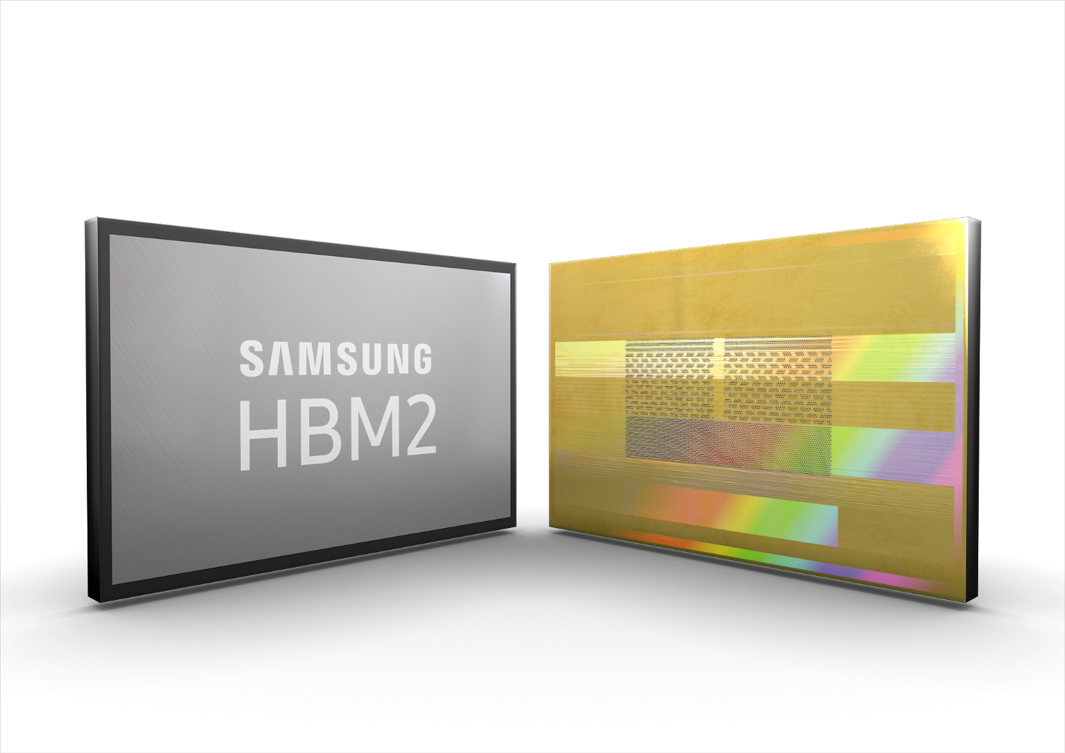
Samsung has increased production of 8GB HBM2 packages to meet emerging market demands. The South Korean company plans to utilize newly finished fabrication facilities to ship more than 50% of its HBM2 in the new 8GB capacity stack by the first half of 2018.
HBM2 came to market in June 2016 in 4GB stacks (4x 1GB die) that deliver up to 256GB/s of bandwidth per die. At the time, GDDR5 could muster only 32GB/s of bandwidth. The massive performance comes from an equally large 4096-bit interface paired with high clock speeds. Nvidia used the previous generation with 4GB in the stack for the $6,000 Quadro GP100 and achieved a record setting 720GB/s of memory bandwidth. The new Tesla V100 increases the overall bandwidth to 900GB/s, but it also uses the smaller 4GB capacity packages.
Increasing the number of die in the package is tricky business. The press release stated:
Article continues belowSamsung’s 8GB HBM2 delivers the highest level of HBM2 performance, reliability and energy efficiency in the industry, underscoring the company’s commitment to DRAM innovation. Among the HBM2 and TSV (Through Silicon Via) technologies that were utilized for the latest DRAM solution, more than 850 of them have been submitted for patents or already patented.
TSV is the new buzz technology for DRAM and NAND flash memories. Instead of using wire bonding on the side of each die, the signals pass through the silicon. Each HBM2 die contains over 5,000 TSVs and over 40,000 in Samsung's new HBM2 8GB product, with eight die connected in a manner that reduces power consumption and temperatures while still guaranteeing high reliability.
At this time we don't know of any product announcements with Samsung's new 8GB high bandwidth memory. The technology will allow GPU makers to build products with more capacity than previous generations. Although it's possible to use HBM in consumer video cards (AMD chose the technology for the R9 Fury X), most of the production has gone into products designed for professional applications. Uses include CAD/CAM, simulation, machine learning, and parallel computing.
In 2018, it may be used to run Crysis.
Get Tom's Hardware's best news and in-depth reviews, straight to your inbox.

Chris Ramseyer was a senior contributing editor for Tom's Hardware. He tested and reviewed consumer storage.
-
Bossman2 Crysis is still a demanding game up to this day. So lets see how this HBM2 stand for itself..Reply -
ClusT3R The only problem is at least in gaming there is not huge difference between one one memory and the other it seems the games runs better in DDR5 than HBM I'm a furyx owner amazing card but i think games does not utilize what this card offer.Reply -
falchard You have to manipulate your settings for HBM. There are some things that favor high memory bandwidth and some things that do not.Reply -
bit_user ReplyThe massive performance comes from an equally large 4096-bit interface paired with high clock speeds.
Should be "low clock speeds", at least relative to GDDR5 and GDDR5X. That's why it needs to be so much wider than traditional GPU memory buses. However, one benefit of the low frequency (and close proximity) is improved power efficiency vs. GDDR5.
