Next-gen MRAM breakthrough can flip bits at SRAM-rivalling speeds with low power consumption — researchers claim true next-gen breakthrough using Tungsten layer
Technology is compatible with existing semiconductor manufacturing methods.

Get Tom's Hardware's best news and in-depth reviews, straight to your inbox.
You are now subscribed
Your newsletter sign-up was successful
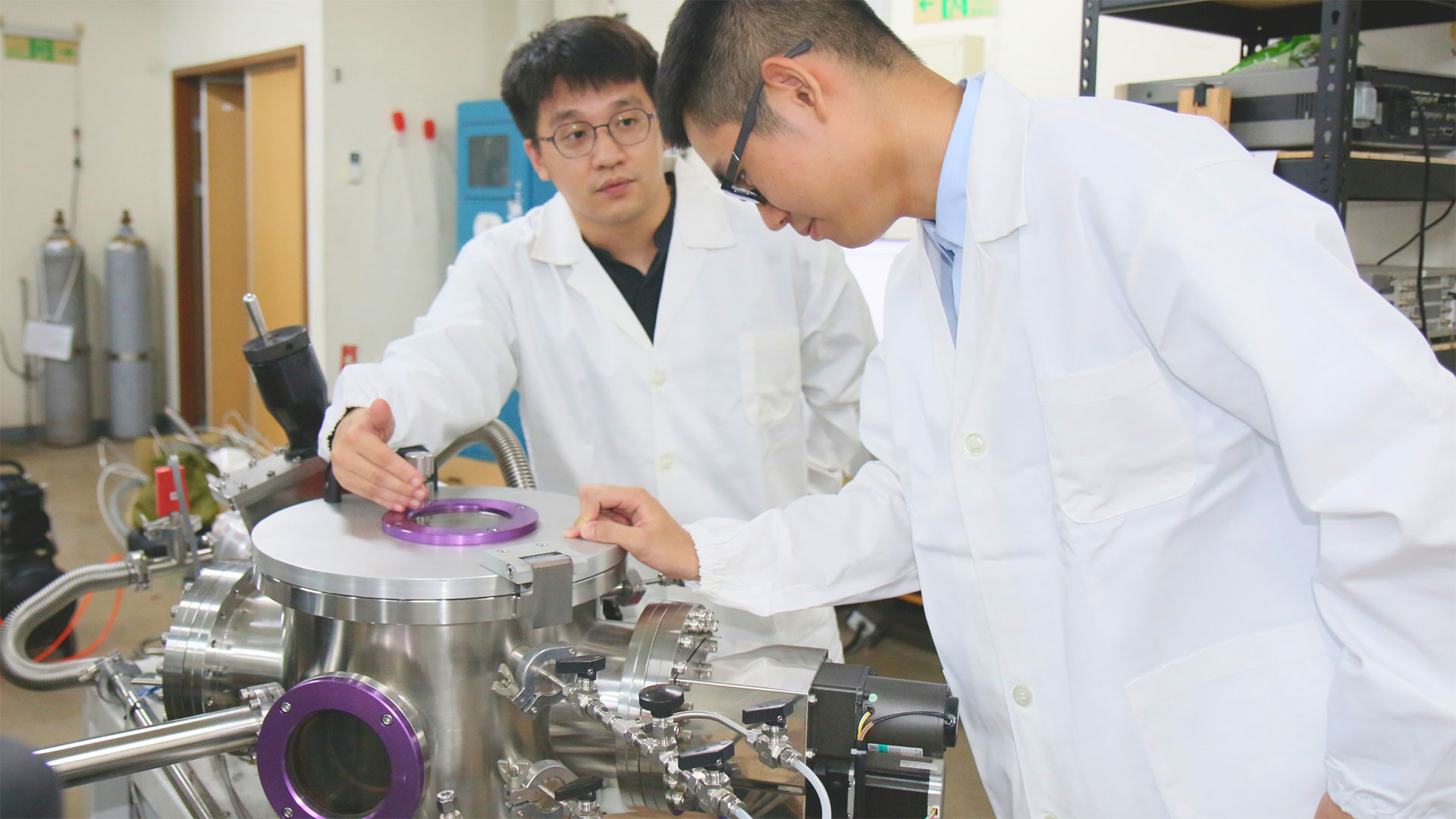
A cross-institutional research team has published a paper where a breakthrough in (MRAM) development is detailed. According to a blog post published by Taiwan’s National Yang Ming Chiao Tung University (NYCU), which spearheaded the efforts, they have managed to overcome a major challenge that hampered the development and adoption of this kind of non-volatile memory. The researchers claim that their spin–orbit torque magnetic random-access memory (SOT-MRAM) is a true next-gen breakthrough as it offers ~1ns switching speeds, and data retention exceeding 10 years, among its multitude of attractions.

This latest SOT-MRAM development comes from a cross-institutional collaboration between Taiwan’s National Yang Ming Chiao Tung University (NYCU), leading chip foundry TSMC, Taiwan’s Industrial Technology Research Institute (ITRI), the National Synchrotron Radiation Research Center (NSRRC) in Taiwan, Stanford University, and National Chung Hsing University (NCHU) in Taiwan. We’ve covered the same team’s earlier advances in building a SOT-MRAM array chip (Jan 2024) but much progress has been made since then.
Tungsten layer
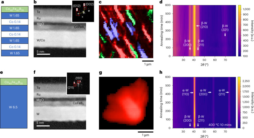
The key advance presented in the recently published paper is the introduction of a tungsten layer to generate the spin currents. Specifically, the team managed to stabilize the rare beta-phase of Tungsten, which is crucial for increased performance – and will be even more important for eventual mass production of SOT-MRAM devices.
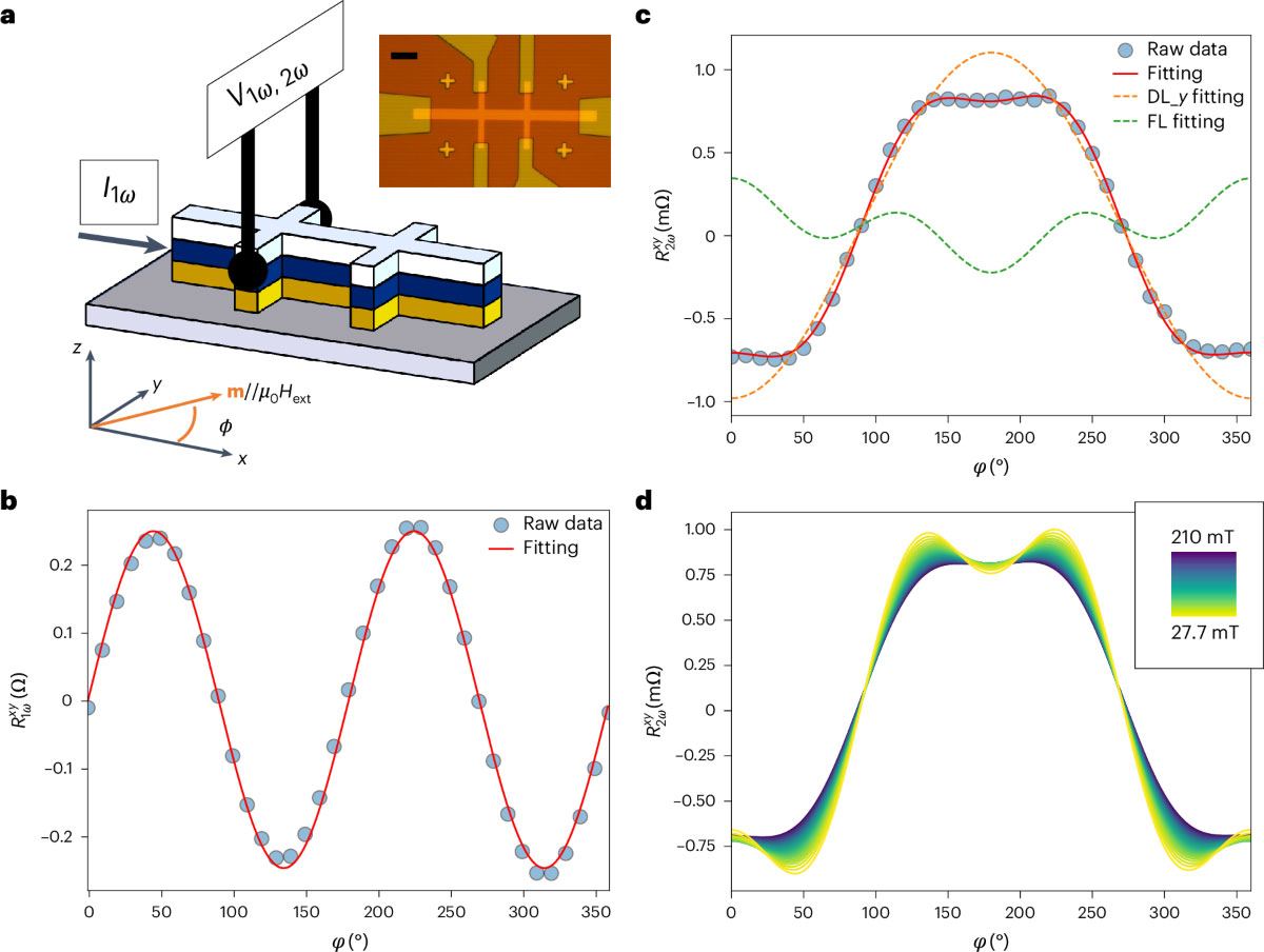
Article continues belowLast year, we noted that NYCU’s SOT-MRAM was capable of latencies up to 10ns. Now it has been improved to ~1ns, rivaling SRAM, reveals testing of a 64kb array the scientists built. For further context, that is slightly faster than DRAM (DDR5 has latency around 14ms) and considerably faster than 3D TLC NAND (which has read latencies between 50 and 100 microseconds).
Don’t forget, though, that this new SOT-MRAM brings the benefits of non-volatility. Other trumpeted advances delivered by the latest SOT-MRAM device demo were:
- Ultrafast switching speeds (as fast as one nanosecond)
- Data retention exceeding 10 years
- A tunneling magnetoresistance of 146%
- Low power consumption, suitable for energy-critical applications
Cobalt too
The research paper reveals that “the insertion of thin layers of cobalt can be used to stabilize β-tungsten under back-end-of-line-compatible thermal conditions.” With the new composite layers, the SOT-MRAM was tested to withstand extreme temperatures (up to 400 °C) for 10 hours, and even 700 °C for 30 mins.
Deliverability and applications
With TSMC scientists among the collaborators, it isn’t surprising to hear that these new SOT-MRAM devices are being designed for large-scale integration under existing semiconductor industry-compatible processes. Almost inevitably, the SOT-MRAM is now being pitched at the AI data center market, as well as low-power computing applications at the edge, where speed and non-volatility will also help spur adoption.
Get Tom's Hardware's best news and in-depth reviews, straight to your inbox.

Follow Tom's Hardware on Google News, or add us as a preferred source, to get our latest news, analysis, & reviews in your feeds.

Mark Tyson is a news editor at Tom's Hardware. He enjoys covering the full breadth of PC tech; from business and semiconductor design to products approaching the edge of reason.
-
cyrusfox Any word on density here? Where are they hoping to disrupt in the current memory hierarchy? The performance and nonvolatile is great, Optane also had that(Although not this fast), issue is price per bit, economy of scales to overcome, and market to adopt and disrupt.Reply
With this having SRAM like performance one would think direct chip attach. As only 56kb has been built, seems a bit far off before it can disrupt much of anything. -
yearswithgpu Oh hey look, another "we're going to get flying cars" type of overhyped piece a tech.Reply
Wake me up when Industry actually FIXES the gen 4,5 SSD heat spike problems other than pasting thermal paste everywhere. -
kerberos_20 Reply
that ARM/ARC processor (storage controller with multiple cores) does alot of processing, which translates into more power draw = more heat, same goes for NAND chipsyearswithgpu said:Oh hey look, another "we're going to get flying cars" type of overhyped piece a tech.
Wake me up when Industry actually FIXES the gen 4,5 SSD heat spike problems other than pasting thermal paste everywhere. -
yearswithgpu Replykerberos_20 said:that ARM/ARC processor (storage controller with multiple cores) does alot of processing, which translates into more power draw = more heat, same goes for NAND chips
I don't like when my overpriced SSD magically jumps to 65c'ish just because I'm using my laptop quite regularly and stays there for about 2mins.
Big tech does not like being criticized and ruin everyone else's daily lives and comments like yours are what Big tech wants. Excuse everything, finding a potential but fake reasoning.
Just my two cents no offense included towards to you -
Findecanor Sounds cool. I wonder how many erase/write-cycles a single cell can take.Reply
All other non-volatile memory technologies I've heard of are more or less limited. Better than Flash, but still. -
kerberos_20 Reply
density is better than SRAM, SOT-MRAM is targeted for CPU cache replacement, not for flash replacementcyrusfox said:Any word on density here? Where are they hoping to disrupt in the current memory hierarchy? The performance and nonvolatile is great, Optane also had that(Although not this fast), issue is price per bit, economy of scales to overcome, and market to adopt and disrupt.
With this having SRAM like performance one would think direct chip attach. As only 56kb has been built, seems a bit far off before it can disrupt much of anything.
i doubt your CPU has only 56kb of SRAM, all the L1,L2,L3 are all SRAM (1bit cells, 2bit cells, etc)...even huge X3D cache is also SRAM
as it goes same for SRAM, optimizing for density means lowering performance, highest density SOT-MRAM has 8GB size (64Gbit) and its speed is slower than DRAM and faster than flash https://www.kioxia.com/en-jp/rd/technology/topics/topics-82.htmlthis one is targeted for memory hungry operations or databases (CSM or CXL) - ie servers -
Steve Nord_ Reply
Decide who you're criticizing and stick with it, the fake reasoning thing really could be explained better, and you really can wrap a foot of copper plate around the bottom of your lappie and in over a SSD or two. And take a pic. and shame say, HP.yearswithgpu said:I don't like when my overpriced SSD magically jumps to 65c'ish just because I'm using my laptop quite regularly and stays there for about 2mins.
Big tech does not like being criticized and ruin everyone else's daily lives and comments like yours are what Big tech wants. Excuse everything, finding a potential but fake reasoning.
Just my two cents no offense included towards to you
Did your nameless laptop need to ship with liquid cooling and a fan or exposed panel for the SSD, or not? This is a Wendy's at NUS (missed the link, actually) where they invent durable cohort storage devices... -
Steve Nord_ Reply
That would suck to get this in 2031 and have someone used to using it say when it needs a Ray-usst. It's a magnetic state, it goes bad when there's a solar flare and you rip off its covers or load it up for a 22T MRI (then try to flip back the manufacturing fuse that blows when it gets any MRI.) Not as dense yet. Also not from a Wendy's at NUS but National Yang Ming Chiao Tung University Hsinchu, Stanford, TSMC, another Hsinchu org (no reason to call it NIST...) and one other place.Findecanor said:Sounds cool. I wonder how many erase/write-cycles a single cell can take.
All other non-volatile memory technologies I've heard of are more or less limited. Better than Flash, but still. -
cyrusfox Reply
The 56kb is in direct reference to the article, yes SRAM is usually much bigger these days (especially L2 and further). 56kb is the total amount the test chip has been demonstrated, a lot of work left to scale up.kerberos_20 said:i doubt your CPU has only 56kb of SRAM, all the L1,L2,L3 are all SRAM (1bit cells, 2bit cells, etc)...even huge X3D cache is also SRAM
This tech I only see viable thus far on a packaged chip (like STT-MRAM offerings) until they can demonstrate more robust manufacturing and yields but with how precise the film composition and exacting thickness required as well as the thermal sensitivity, I doubt we will see this replacing robust SRAM anytime soon. -
bit_user Reply
This.cyrusfox said:Any word on density here? Where are they hoping to disrupt in the current memory hierarchy?
I don't even care how fast it is, unless it can scale down to densities that are competitive with the use of SRAM, in modern CPU and GPU-class chips.
The first test is whether it can challenge SRAM. Modern 3D NAND is way more dense.cyrusfox said:The performance and nonvolatile is great, Optane also had that(Although not this fast), issue is price per bit, economy of scales to overcome, and market to adopt and disrupt.
Without telling us the physical dimensions that array is, such a size figure is pretty meaningless (other than simply to show that it can be used in memory-like configurations).cyrusfox said:As only 56kb has been built,

