Researchers achieve breakthrough integration of 2D materials on standard silicon chips
Researchers at Fudan University have created a working memory chip just a few atoms thick.

Get Tom's Hardware's best news and in-depth reviews, straight to your inbox.
You are now subscribed
Your newsletter sign-up was successful
For the first time, scientists have successfully built a fully functional memory chip using two-dimensional materials and integrated it directly onto a conventional silicon die — a milestone that could change how future semiconductors are made. The research, led by Chunsen Liu and colleagues at Fudan University in Shanghai, was published on October 9 in the journal Nature.
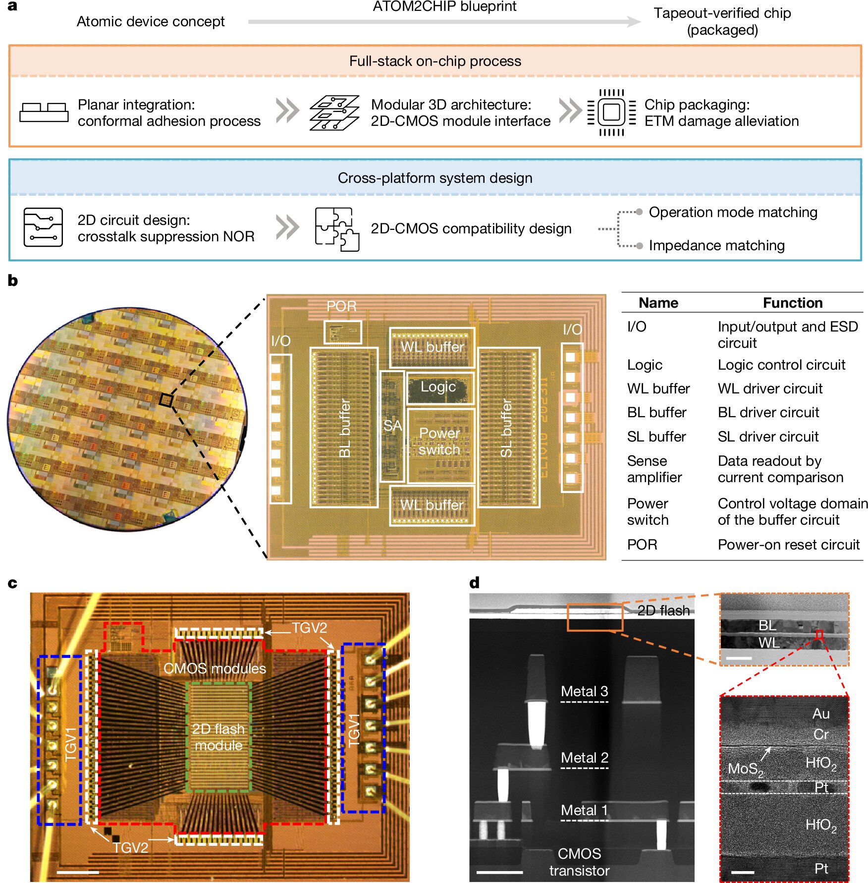
The research may mark a turning point for 2D electronics, which have long promised atomic-scale performance and efficiency but struggled to move beyond lab demonstrations. Using a process the team calls ATOM2CHIP, the researchers grew a layer of molybdenum disulfide just a few atoms thick directly on top of a conventional 0.13-micrometer CMOS silicon chip. The result is a hybrid chip that combines a 2D NOR flash memory array with a standard CMOS controller, effectively bridging the gap between experimental nanomaterials and industry-standard fabrication.
The Fudan team reports a 94.34% yield from full-chip testing — a figure that rivals commercial silicon production — and operational speeds up to five megahertz. Each bit consumes just 0.644 picojoules, far below the energy draw of today’s silicon flash cells. The memory demonstrated fast 20-nanosecond programming and erasing, ten-year data retention, and endurance of over 100,000 write cycles.
Article continues belowTo achieve this, the researchers had to overcome the challenge of surface roughness. Silicon chips, even after polishing, have uneven terrain at the nanometer scale that can tear or stress atomic-thin layers. The ATOM2CHIP method introduced a conformal adhesion process that allows the 2D material to “flow” over the contours of the underlying circuits without breaking, while a 2D-friendly packaging system guards against heat and electrostatic damage.
Equally crucial was the team’s “cross-platform system design,” a custom interface ensuring the 2D layer could communicate seamlessly with the CMOS control logic. This design enables instruction-driven operations, 32-bit parallelism, and random access, or, in other words, a full-featured memory chip.
In their paper, the authors describe the result as “an important milestone in extending the superiority of 2D electronics to real-world applications.” The implications go well beyond flash storage. If scaled, such hybrid architectures could drastically reduce power use and increase density in next-generation processors and AI processors, effectively continuing Moore’s Law at the atomic limit. While mass production is still years away, this is the closest 2D materials have come to commercial relevance.

Follow Tom's Hardware on Google News, or add us as a preferred source, to get our latest news, analysis, & reviews in your feeds.
Get Tom's Hardware's best news and in-depth reviews, straight to your inbox.

Luke James is a freelance writer and journalist. Although his background is in legal, he has a personal interest in all things tech, especially hardware and microelectronics, and anything regulatory.
