Tom's Hardware Verdict
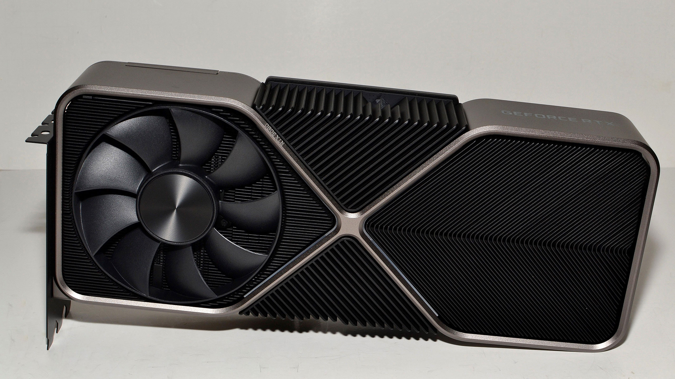
Nvidia's GeForce RTX 3090 Founders Edition takes the crown as the fastest GPU around, but at twice the price of an RTX 3080. It's blazingly fast, comes with gobs of memory, and the Founders Edition is absolutely massive … and most gamers don't need it. We discuss price, performance, availability, power, and more in our in-depth review.
Pros
- +
Fastest current graphics card, period
- +
4K ultra at more than 60 fps
- +
8K DLSS potential
- +
Good cooling and minimal noise
- +
Major architectural updates for the future
- +
Great for content creation tasks
Cons
- -
Extreme pricing for very modest gains
- -
Massive cooler won't fit in smaller builds
- -
Lacks certain Titan features
- -
Highest TGP for a single GPU ever (350W)
- -
Needs a 4K display, maybe even 8K
Why you can trust Tom's Hardware
The Nvidia GeForce RTX 3090 Founders Edition now claims the top spot on our GPU benchmarks hierarchy, though where it lands on the best graphics cards is a more difficult question to answer. While the GeForce RTX 3080 kept with the existing pricing structure of the RTX 20-series, replacing the RTX 2080 Super at the $699 price point, the RTX 3090 sees the RTX 2080 Ti's $1200 launch price and raises it another $300. There's an alternative viewpoint, however: The GeForce RTX 3090 is also a replacement for the $2,500 Titan RTX, in which case it's a faster card that costs $1,000 less. Either way, you're going to need some deep pockets if you want to own Nvidia's new halo card.
We already have the Ampere architecture deep dive that details what makes the GeForce RTX 3090 tick. Start there if you want more information on how the 3090 and GA102 deliver new levels of performance. We'll cover the highlights here, but the simple answer is that Nvidia has gone with a smaller process node, more cores, faster memory … plus more power and a higher price. At 350W TGP (Total Graphics Power), this is by far the most power hungry consumer GPU Nvidia has ever released (not counting the dual-GPU cards). It's also the most expensive GeForce branded GPU ever (unless you count the dual-GPU GeForce GTX Titan Z, which I don't).
We have a few additional tests we're still trying to run before we render our final verdict (looking at you 8K, or at least 4K with DSR emulating 8K), so we won't have a final verdict just yet. We also have a few AIB (add-in board) partner cards that we'll be looking at in the coming days, once we've had some time to run all the tests and gather some data.
One thing we can't fully predict is availability, but our hunch is that it's not going to be great. It's actually more than a hunch, now, as Nvidia pre-emptively apologized yesterday for the limited availability of RTX 3090 cards (while at the same time confirming performance expectations). Ugh. Considering the RTX 3080 cards have been selling out as fast as inventory arrives, even though the RTX 3090 costs over twice as much … well, some people are paying nearly $1,500 for RTX 3080 cards. It's probably not going to be pleasant if you have your heart set on a 3090 and didn't put in a pre-order. Just give it some time, and things should eventually get sorted out. Cue mom: "Patience is a virtue!" Thanks, ma, but I'm still working on it.
The short summary of the GeForce RTX 3090 is much as you'd expect. It's theoretically about 20% faster than the RTX 3080 based on specs alone, with over twice the memory. The extra VRAM doesn't really matter much for most games unless you're running at 8K (maybe 5K), but it can prove useful for some professional workloads. The RTX 3090 also requires a beefy CPU to get the most out of the card (we'll be running some additional tests in the coming days to show that, but you can get some idea of what to expect from our RTX 3080 CPU scaling article). This is very much a GPU designed for 4K ultra gaming, and at those settings, it's 12% faster than the 3080 on average in our existing test suite, and 14% faster in our bonus test suite. Drop down to 1440p ultra, and the 3090 is only 8% faster than the 3080. If you're running at 1080p? Don't bother, seriously.
Now, let's dig into the specs and look at what's changed relative to other Nvidia GPUs.
Nvidia GPU Specifications
| Graphics Card | RTX 3090 FE | RTX 3080 FE | Titan RTX | RTX 2080 Ti FE |
|---|---|---|---|---|
| Architecture | GA102 | GA102 | TU102 | TU102 |
| Process Technology | Samsung 8N | Samsung 8N | TSMC 12FFN | TSMC 12FFN |
| Transistors (Billion) | 28.3 | 28.3 | 18.6 | 18.6 |
| Die size (mm^2) | 628.4 | 628.4 | 754 | 754 |
| SMs | 82 | 68 | 72 | 68 |
| GPU Cores (FP32) | 10496 | 8704 | 4608 | 4352 |
| GPU Cores (INT32) | 5248 | 4352 | 4608 | 4352 |
| Tensor Cores | 328 | 272 | 576 | 544 |
| RT Cores | 82 | 68 | 72 | 68 |
| Base Clock (MHz) | 1395 | 1440 | 1350 | 1515 |
| Boost Clock (MHz) | 1695 | 1710 | 1770 | 1635 |
| VRAM Speed (Gbps) | 19.5 | 19 | 14 | 14 |
| VRAM (GB) | 24 | 10 | 24 | 11 |
| VRAM Bus Width | 384 | 320 | 384 | 352 |
| ROPs | 112 | 96 | 96 | 88 |
| TMUs | 328 | 272 | 288 | 272 |
| TFLOPS FP32 | 35.6 | 29.8 | 16.3 | 14.2 |
| TOPS INT32 | 17.8 | 14.9 | 16.3 | 14.2 |
| Tensor TFLOPS FP16 (Sparsity) | 142 (285) | 119 (238) | 130 | 114 |
| RT TFLOPS | 69.5 | 58.1 | 49.2 | 45.7 |
| Bandwidth (GBps) | 936 | 760 | 672 | 616 |
| TDP (watts) | 350 | 320 | 285 | 260 |
| Launch Date | September 2020 | September 2020 | December 2018 | September 2018 |
| Launch Price | $1,499 | $699 | $2,499 | $1,199 |
GeForce RTX 3090 Architecture: Nearly a Full GA102
Again, our Ampere architecture goes into more detail on the various aspects of the new 30-series GPUs. There are a lot of changes relative to the previous Turing architecture, but here's the highlight reel.
Get Tom's Hardware's best news and in-depth reviews, straight to your inbox.
First, GA102 uses Samsung's 8N process technology, which means more transistors in a smaller area than TU102. Looking strictly at overall transistor density, GA102 packs in 45 million transistors per square millimeter, whereas TU102 density is 'only' 24.7 million transistors per square millimeter. That's good, but clearly not as good as TSMC's N7 node: The larger GA100 chip used in Nvidia's A100 contains 65.4 million transistors per square millimeter. Also, AMD's Navi 10 has 41 million transistors per square mm, so Nvidia has at least matched that level of density — comparing across architectures is definitely looking at apples and oranges, though.
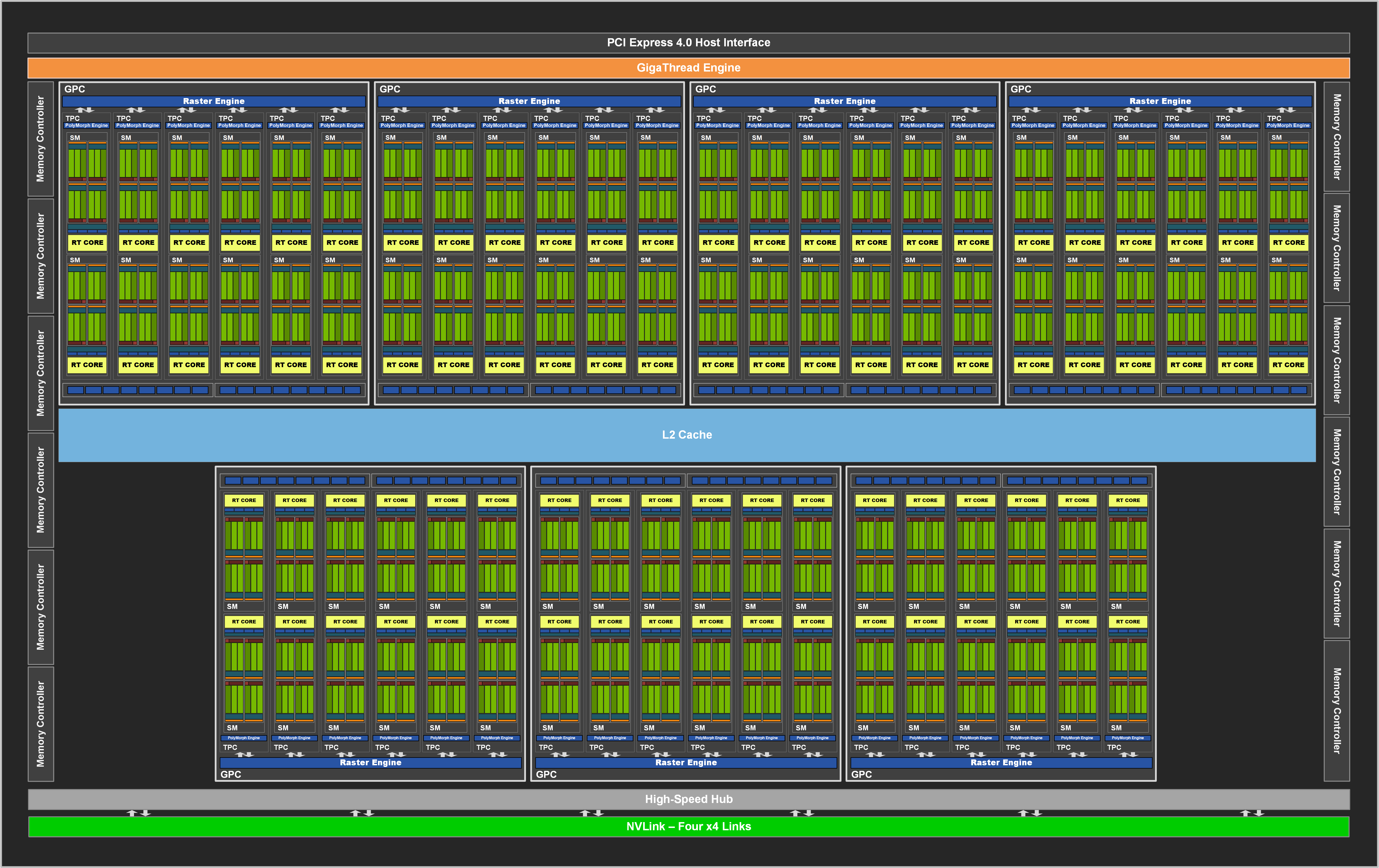
Moving on, the GeForce RTX 3090 uses a nearly complete GA102 chip. Of the 84 potential SMs (streaming multiprocessors), only two are disabled. That suggests either the yields are very good … or Nvidia isn't planning to sell nearly as many 3090 chips as 3080 chips. We suspect the second option is closer to the truth, and actual yields are a closely guarded secret these days. The 3090 also has seven GPCs (graphics processing clusters), and the ROPs (render outputs) are now part of the GPC instead of the memory controller, giving the 3090 112 ROPS.
Perhaps a bigger change is that the GeForce RTX 3090 comes equipped with 24GB of GDDR6X memory, this time clocked at 19.5 Gbps (compared to 19 Gbps on the 3080). This is accomplished by enabling the final two 32-bit memory controllers on GA102, and then running 24 chips in half-width 16-bit interface mode. That also means the GDDR6X chips are located on both sides of the PCB (printed circuit board), whereas the RTX 3080 only has memory on the same side as the GPU. There's certainly a question of how much this affects GDDR6X memory temperatures, particularly when half the VRAM isn't actively cooled. However, at present, we don't have a way to measure the GDDR6X chip temperatures.
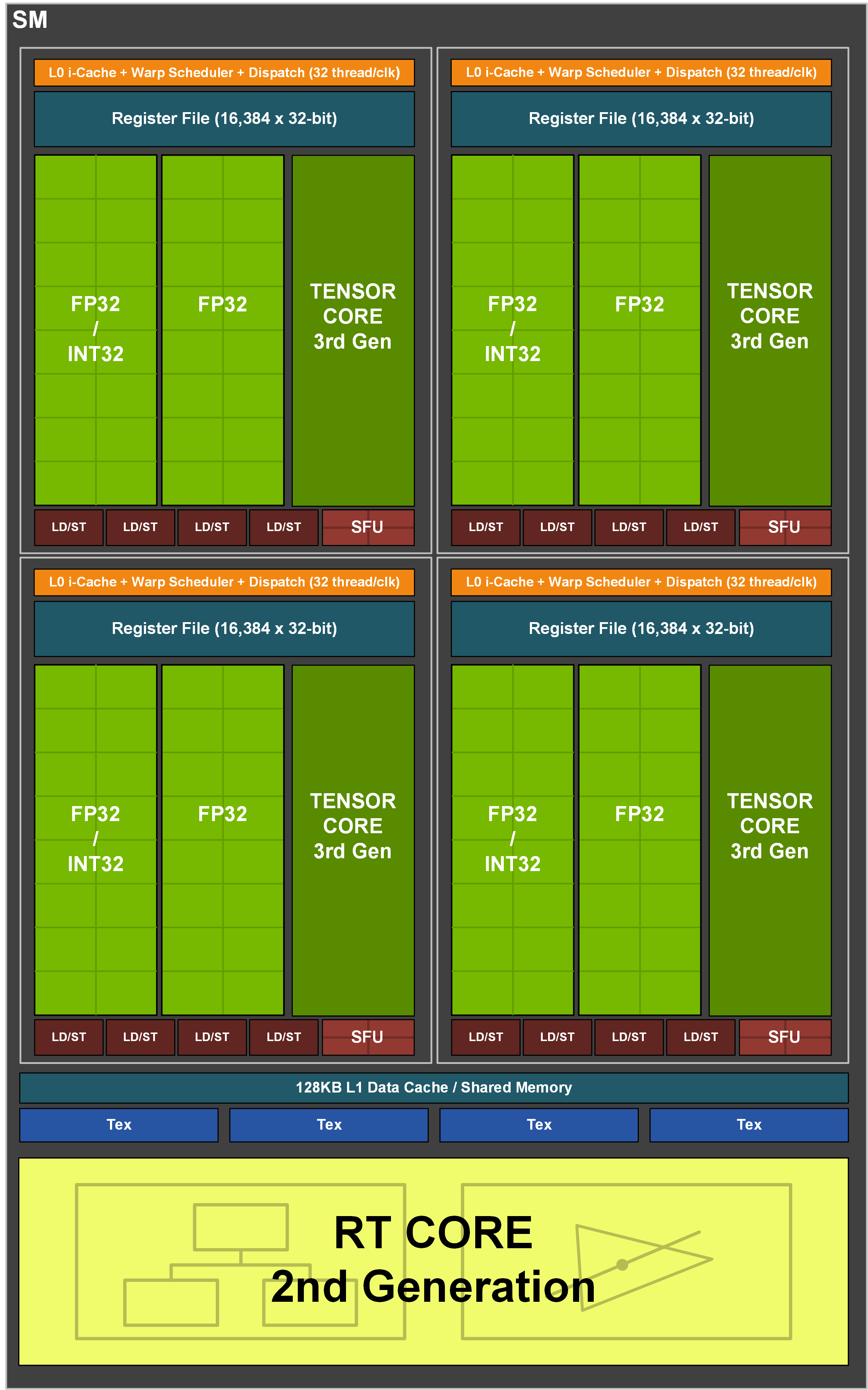
We've discussed the GPU CUDA core changes quite a bit in previous Ampere articles, because it's one of the most significant differences between Ampere and Turing. Turing included 64 FP32-capable CUDA cores per SM, with an additional 64 INT32-capable CUDA cores (and two FP64 cores for compatibility purposes). The FP32 and INT32 cores were separate datapaths and could be used concurrently. The FP32 cores could also run FP16 math at double the performance — 'fast math' mode.
For Ampere, the FP32 cores lose support for FP16 fast math, which gets shifted over to the Tensor cores — it's still twice the FP16 performance of the dedicated FP32 cores, but only equal FP16 performance overall. Meanwhile, the INT32 cores gain support for FP32 calculations, which means total FP32 performance per SM has doubled. At the same time, INT32 performance per SM has stayed the same. This has some interesting ramifications for overall performance, but basically, about 30-35% of the CUDA core workload in games is INT32 (for address pointer lookups, texture calculations, and other similar work). That means a good chunk of the second datapath will be busy with INT32, so the real-world performance boost will often be less than the raw FP32 TFLOPS number would suggest.
Elsewhere, the tensor cores are another substantial upgrade relative to Turing, with twice the throughput per core. Except there are half as many tensor cores per SM. The 3rd generation tensor cores do add support for fine-grained sparsity, which can double throughput again relative to Turing when used. Also worth noting is that the 3rd gen tensor cores add support for INT8 and INT4 data types at 2x and 4x the base FP16 throughput.
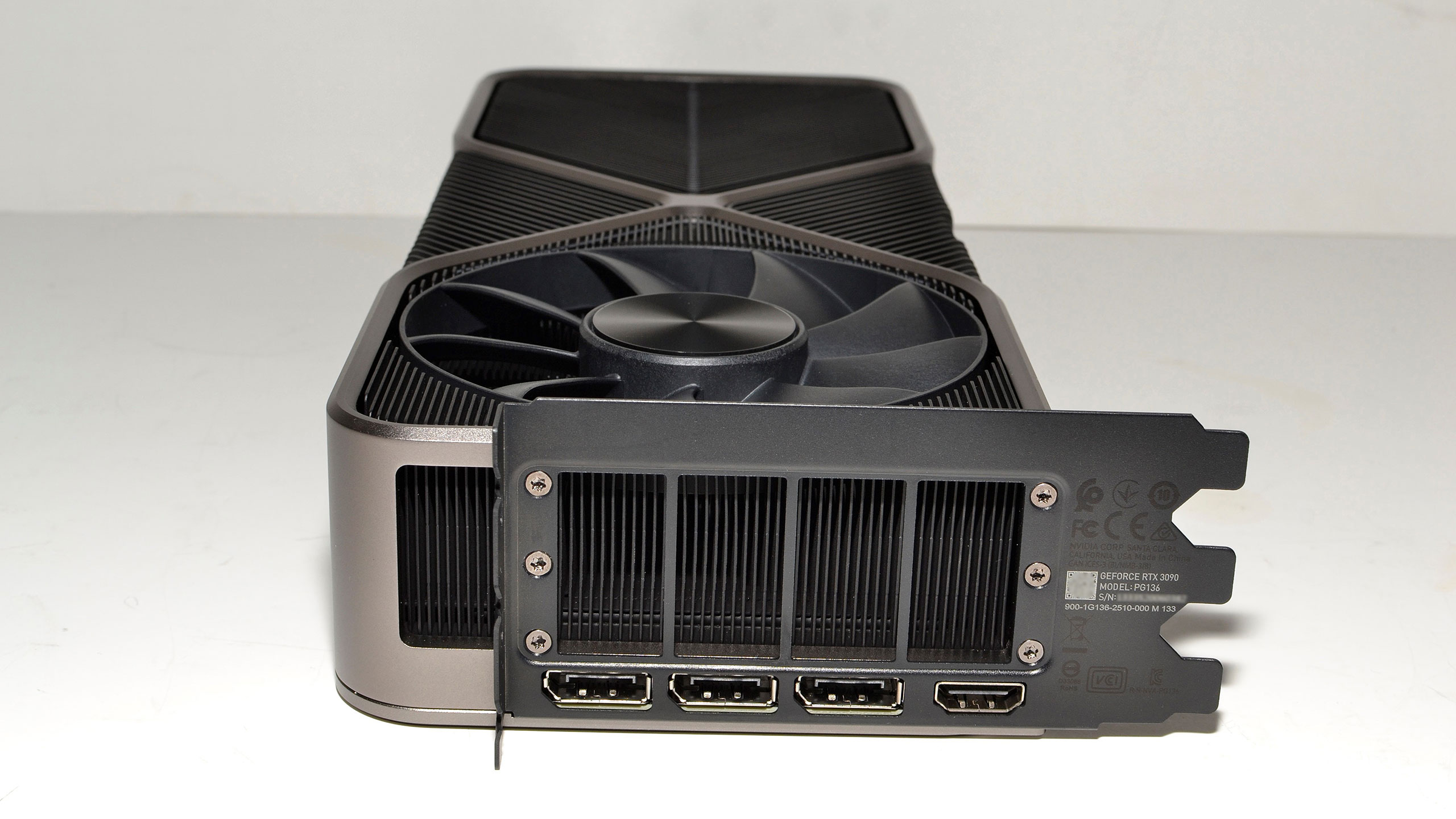
The video ports on GeForce RTX 3090 FE are the same as on RTX 3080: one HDMI 2.1 port and three DisplayPort 1.4a outputs. There's no VirtualLink port this round, as VirtualLink is basically dead. All four outputs are capable of 8K60 using DSC (Display Stream Compression), a "visually lossless" technique that's actually not really visually lossless (though you probably won't notice at 8K). We've seen other cards with five display outputs, many opting for dual HDMI 2.1, so keep that in mind if you're planning to use a multi-monitor setup.
Other changes (and we're glossing over things here as we've already covered this in the RTX 3080 review, as well as the Ampere architecture piece) include RT cores that are up to twice as fast — or even more in certain workloads (like motion blur). The L1 cache/shared memory capacity and bandwidth have been increased. The L2 cache is also larger than before, and the L1 cache can be configured as varying amounts of L1 vs. shared memory, depending on the needs of the application. Register file size is also increased, and GA102 can do concurrent RT + graphics + DLSS (previously, using the RT cores would stop the CUDA cores).
The raster operators (ROPS) have been moved out of the memory controllers and into the GPCs. Each GPC has two ROP partitions of eight ROP units each. This provides more flexibility in performance, giving the GA102 and RTX 3090 a total of 112 ROPS. Each GPC also includes six TPCs (Texture Processing Clusters) with eight TMUs (Texture Mapping Units) and a polymorph engine, though these come in pairs and Nvidia enables 41 TPCs for the 3090.
Finally, as discussed before, the RTX 3090’s memory controller has a new feature called EDR: Error Detection and Replay. When the memory detects a failed transmission, rather than crashing or corrupting data, it simply tries again. It will attempt to do this until successful, though it's still possible to cause a crash with memory overclocking. EDR allows the potential for higher memory clocks that may not actually perform better as you approach the limits of the memory. That's because EDR ends up reducing total memory throughput when failed transmissions occur.
Current page: GeForce RTX 3090 Founders Edition: An Absolute Unit
Next Page GeForce RTX 3090 Founders Edition: Design, Cooling, Aesthetics
Jarred Walton is a senior editor at Tom's Hardware focusing on everything GPU. He has been working as a tech journalist since 2004, writing for AnandTech, Maximum PC, and PC Gamer. From the first S3 Virge '3D decelerators' to today's GPUs, Jarred keeps up with all the latest graphics trends and is the one to ask about game performance.
-
VforV "Titan-class card" - again with this nvidia BS?Reply
It's not, it's a catchphrase from nvidia and the media keeps playing this tune. It's only a more expensive 3080 Ti, which will be proven soon. A halo product for people with more money than sense.
"Fastest current graphics card, period" - Wrong, it's not, it's based on the game and if it's optimized for nvidia (DLSS) or AMD (and no DLSS). In the first case it wins in the latter one it gets beaten by RX 6800 XT and RX 6900 XT, sometimes by a mile... as much as it beats them in the first case with DLSS ON, but then AMD does it by raw power. So it's 50/50, period.
"8K DLSS potential" - yeah, sure "potential". If you count dreaming of 8k gaming potential too, then yes. Again nvidia BS propagated by media still.
"Needs a 4K display, maybe even 8K" - no it does not "need" an 8k display unless you want to be majorly disappointed and play at 30 fps only. That is today, with today games and today's graphics demands, but tomorrow and next gen games you can kiss it goodbye at 8k. Another nvidia BS, again supported by the media.
GJ @ author, nvidia is pleased by your article. -
Loadedaxe Titan Class card? No offense, but to Nvidia it is. The rest of the world its a 3080Ti.Reply -
HideOut Mmmm 2 months late for a review? Whats happened to this company. Late or missing reviews. Nothing but rasberry Pi stuff, and sister publication anantech is nearly dead.Reply -
Blacksad999 Reply
Yeah, the Raspberry Pi stuff is getting annoying. They brought out their 5800x review way after the fact, too. Kind of odd. I understand it's a difficult year to review things, but months later than most review sites isn't a good look when that's supposed to be the sites specialty.HideOut said:Mmmm 2 months late for a review? Whats happened to this company. Late or missing reviews. Nothing but rasberry Pi stuff, and sister publication anantech is nearly dead.


