P55 On Boost: Five LGA 1156 Boards Between $200 And $250
EVGA P55 FTW
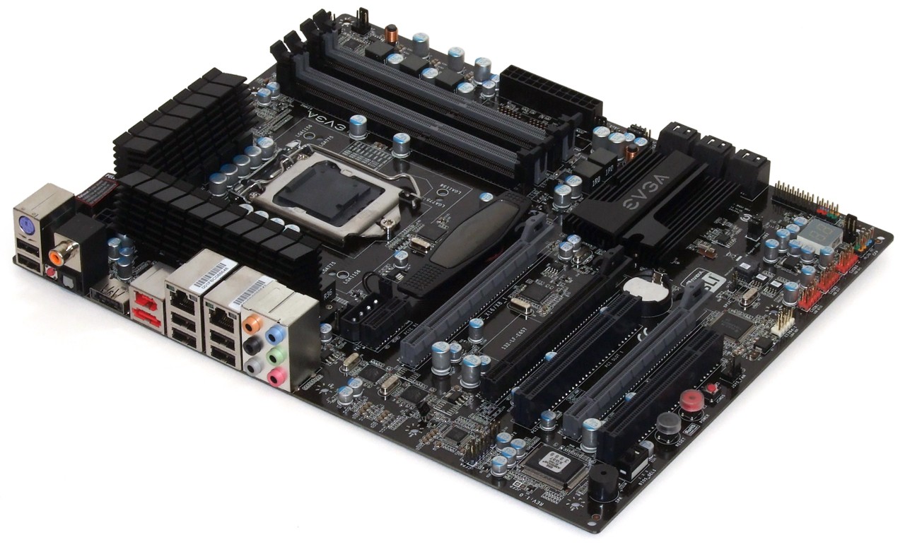
With a Web price starting at around $200, EVGA’s P55 FTW makes incremental improvements compared to its previously tested P55 SLI without breaking the bank.
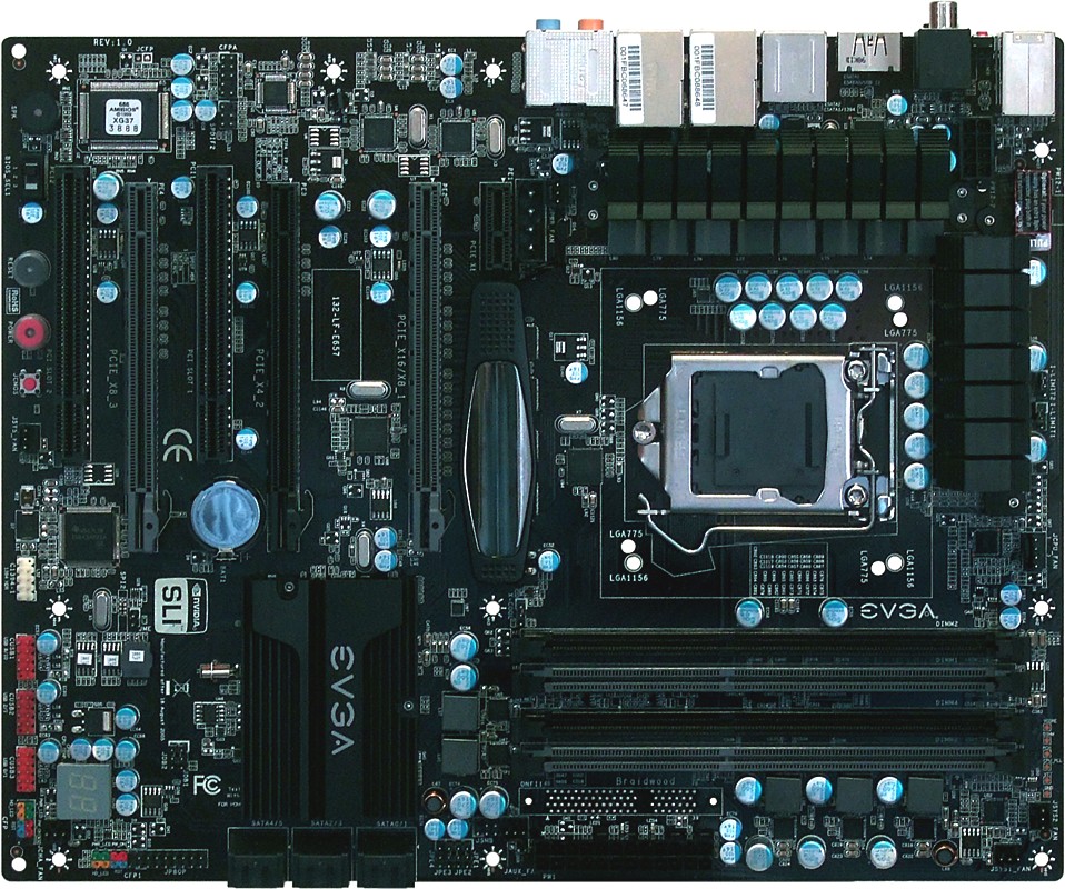
As a board marketed primarily towards overclockers, the biggest advancement of the P55 FTW might be its 14-phase CPU power regulator that EVGA rates at 600W peak output. That’s more than even an eight-pin CPU power connector can supply, so EVGA also adds a second eight-pin EPS12V connector.
While the P55 FTW look nearly identical to its less expensive sibling, the biggest change hardcore gamers will notice is the slot order. SLI and CrossFire come to the LGA 1156 processors by splitting their 16 PCIe 2.0 lanes across two slots, and EVGA rearranges those slots so that they are four spaces apart. Unlike the P55 SLI, the P55 FTW puts the four-lane x16 slot in the middle, so that SLI and CrossFire users who need only graphics cards will get the maximum cooling space between them.
EVGA is the only company in today’s roundup to support both LGA 1156 and LGA 775 coolers, giving extreme-overclocking gurus a great reason not to modify their custom LN2 pots or oversized water blocks. LGA 1156 has a slightly shorter installation height that prevents solid-mount LGA 775 coolers, such as Swiftech’s Apogee Drive, from providing proper contact pressure, so the second set of mounting holes should only be used with spring-loaded mounting mechanisms.
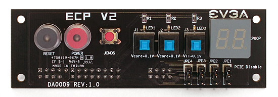
EVGA includes a gadget called EVGA Control Panel Version 2 (ECP V2) that extends several motherboard features beyond the motherboard’s surface via cables. Included are power, reset, CLR_CMOS, two core-voltage, and one uncore-voltage (labeled VTT) buttons, a numeric status display, and a set of jumpers for disabling individual PCIe slots. Each voltage button adds 100mV when engaged. That last feature is supposed to be handy in case an overclocked video card prevents a system boot, but what isn’t as handy is that the module itself has no provisions for front-panel mounting.
Other than the changes noted above, there isn’t much to say about the P55 FTW that hasn’t already been said of the P55 SLI in its review. Both boards strive to be nearly legacy-free, yet both include a single PS/2 port that we still occasionally use, and with the exception of the altered slot order, both have the same layout.
BIOS
Get Tom's Hardware's best news and in-depth reviews, straight to your inbox.
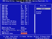
The P55 FTW continues EVGA’s good overall BIOS layout while adding more reference- and signal-voltage controls. The bottom of the frequency/voltage controls page features a menu for saving custom configurations to a protected portion of the BIOS IC as any of four user profiles.
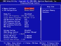
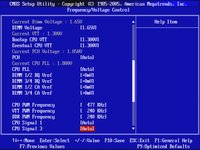
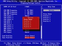
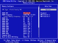
Automatic configuration per setting eases the alteration of the most familiar memory timings.
Accessories
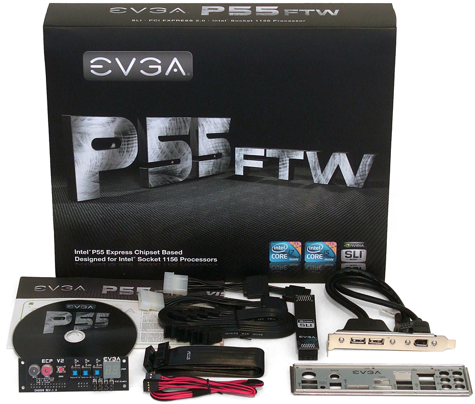
EVGA includes four SATA cables and a single SLI bridge in an installation kit that stands out mostly for its control module.
-
liquidsnake718 Always the question in mind. Is it possible for the manufacturers to make a P55 with FULL SLI 16x 16x? I wouldn’t know. I do know tests have proven that the difference in a 8x, 8x isnt all that bad but If I were going to invest next year on a motherboard Id want the best possible one for the best possible "upgradability".Reply
Also for just $50 more one could get a reasonable X58 board and the core i7 920 would be a great buy. The only motherboard here that would be a "smart" buy with "long term" in mind would be the Gigabyte UD6 since it at least sports USB3.0 AND Sata 6.0. One would not need to purchase any expansion card for this feature as it will be used in the years to come. Also knowing that X58 will be used for 6core chips way ahead is comforting as these boards then will still be around and mainstream by the time those processors will even be relevant for avid/regular PC users.
I just have a few questions you may be able to answer, do you guys also choose motherboards from other countries? I have seen Foxconn and Emaxx in some reviews but I also know that they may not be the best quality boards but it would be great to compare those boards as well. Its also good that you placed a reference Intel P55 so people would know the standard in which to compare with. Also how come we still dont have a P55 or X58 XFX board? Has XFX stopped making mb's and only started to focus on GPU's?
-
nerrawg liquidsnake718"Is it possible for the manufacturers to make a P55 with FULL SLI 16x 16x? I wouldn’t know."Reply
In the article first page:" Can any LGA 1156 system truly be considered high-end? After all, there’s no practical way to supply two graphics cards with a full 16 lanes of bandwidth. However, only the most expensive graphics cards need more than eight PCIe 2.0 lanes, and not every high-end buyer wants a gaming system."
The reason for this is the GPU - CPU bridge on core i5 systems, which in previously intel boards was part of the southbridge chipset, is now integrated onto the CPU. Therefore it isn't the boards that limit GPU lanes to a maximum of x16 lanes total, but it is the p55 core i5 & i7 CPUs that do this.
Check this link for more on the CPU-motherboard layout:
http://www.tweaktown.com/articles/2920/intel_s_p55_express_lynnfield_chipset_overview/index2.html -
I not quite agree with Gigabytes UD6 being the best choice with "long term" in mind. If using USB3.0 or SATA3, your VGA will run at 8x PCIe 2.0 instead of 16x. That might not be a problem with mainstreamcards, but would you rather have your high end GTX295, R5870 or R5970 run at 8x or 16x? I know what I want when buying a topdog card.Reply
Also see this artice on VR-Zone which explains the pitfalls of Gigabytes USB3/SATA3 implementation: http://vr-zone.com/articles/gigabyte-p55a-boards-usb3-sata3-issues-analysis/8158.html -
tacoslave the 8x pci was the only thing that kept me from buying an i5 but instead i got a phenom II 955 and never looked back and i got a great deal with a bundle from newegg. gotta love em.Reply -
kumaiti I would like to suggest a little more depth on the software features of each board. Performance tests are nice and everything but the differences are so small that often the features are the main deciding factor on getting a Mobo. It would be nice to know, for example, which boards support Dolby Digital Live.Reply -
Crashman kumaitiI would like to suggest a little more depth on the software features of each board. Performance tests are nice and everything but the differences are so small that often the features are the main deciding factor on getting a Mobo. It would be nice to know, for example, which boards support Dolby Digital Live.Reply
Good point, perhaps the features comparison chart could be expanded a little. -
apache_lives 1156 platform is mid-range, if you want the full 16x + 16x you go for 1366 its that simple, and nativly there are not enough lanes for dual 16x slots btw and nvidia chips can open them up to almost 16 16 but no real benifit anyhowReply
who would buy a Phenom II rig to get 16 16? not comparing AMD but you would see better performance from a high model i5 with 8 8 lol good one -
donkeykong2009 It will be great to see the performance impact on the Games for the Gigabyte board when USB 3.0 and SATA 3 is enabled.Reply -
Crashman donkeykong2009It will be great to see the performance impact on the Games for the Gigabyte board when USB 3.0 and SATA 3 is enabled.Reply
You can't enable USB 3.0 and SATA 6.0 Gb/s at the same time. -
I'm not talking about full speed CrossFireX or SLI at two times 16x PCIe speed. I'm talking about single VGA solutions. I want my HD5970 to run at fullspeed 16x PCIe express and that's not happening if I connect a USB3 or SATA3 device. Even in single VGA setups, the speed will be cut in half on my PCIe 16x slot to 8x.Reply
I'd rather have the ASUS or MSI (GD85) solution who use an additional PLX chip. The question was about being future proof and the Gigabyte solution is not as future proof as it seems.
Unfortunately Intel seems to be steering away from the X58 platform. There are more and more P55 motherboards coming out which have high end features. The top end Lynnfield CPUs have no problem outrunning the lower end Bloomfield CPUs. So saying a 1156 is midrange... that's giving it less credit than it deserves.
Btw, there are P55 mainboards from ASUS, MSI and EVGA with an NF200 chipset which do offer fullspeed dual CrossFire/SLI at 16/16. And those definitely don't have midrange prices. :o
