When Size Really Matters: Smallest Flash Cards
Get Tom's Hardware's best news and in-depth reviews, straight to your inbox.
You are now subscribed
Your newsletter sign-up was successful
Flash Memory: Here's How It Works
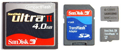
Size comparison: CF and SD are a little too bulky for small mobile devices.
The benefits of flash memory - or, more precisely, Flash-EEPROMs (Electrically Erasable Programmable Read-Only Memory) - are easy to enumerate. They provide a shock insensitive, non-volatile form of data storage that maintains its contents when powered off. Its energy requirements are miniscule, and its memory chips are small, light, and relatively inexpensive.
Although flash memory can be used like static RAM (SRAM), writing to such stores is trickier: that's because addressing and access are more complicated, and erasing memory contents doesn't work byte-wise. That explains why writing to flash memory is always much slower than reading its contents.
An often untold story about flash memory is the limited number of write cycles it tolerates. That's because electrical charges provide permanent retention of transistor states. These charges are isolated by oxide layers, which help maintain consistent state, but also dissipate over time. Semiconductor makers claim as many as 100,000 write cycles for flash memory, but a little skepticism is probably well-advised.
One can also distinguish between NOR and NAND types of flash memory, which refers to how these memory cells actually work. NOR flash is linearly addressable using a conventional processor, and thus also works for delivering executable code. But it's also slower than NAND, and requires more energy to read and write, explaining why it's used primarily for burning and accessing programs in firmware.
All the memory devices we cover in this article use NAND flash. It offers faster performance, consumes less power, scales well - which explains how 4 and 8 GB products are possible - and works from a command-based bus interface. But memory controller overhead is higher and more complex, and conventional processors require translation routines to mediate, enabling them to read from and write to NAND flash memory.
NAND flash may be further distinguished between Multi-Level-Cell and Single-Level-Cell architectures (MLC, SLC). This notion of level is logical rather than physical. A single MLC cell offers two bits and thus four possible states to store data: erased (empty), one third, two thirds, and fully programmed. This leads to performance consequences compared to SLC, which offers only one bit and two states for each memory cell. SLC is simpler, faster, and also saves energy. Also, the higher energy consumption involved in handling bits pairwise leads to quicker dissipation of the oxide layers between individual memory cells. That's why MLC is rated only for a maximum of 10,000 write cycles.
Get Tom's Hardware's best news and in-depth reviews, straight to your inbox.
Implementing SLC logic is more complex, which makes such chips more expensive. Because of its noticeably higher performance and longevity, SLCs are conquering the market because of their noticably higher performance and longevity and certainly will continue to dominate.
Current page: Flash Memory: Here's How It Works
Prev Page The Midgets Are Coming! Next Page Too Big? Compact Flash
Patrick Schmid was the editor-in-chief for Tom's Hardware from 2005 to 2006. He wrote numerous articles on a wide range of hardware topics, including storage, CPUs, and system builds.
