Inside Western Digital: How Tomorrow's Storage Gets Made
Will It Glide?
With disks now encased in multiple sputter layers, it’s time to see if WD’s process is yielding proper surface characteristics. With areal densities now at several hundred gigabits per square inch, the magnetic head has to “fly” above the disk surface at a height of one micro-inch (one-millionth of an inch) or less. Therefore, any bumps on the disk surface can cause a “head crash,” wherein the head plows into the media and gouges a track in it, potentially wiping out data and destroying the drive. Similarly, a divot of just 10 nanometers in the surface can result in missing bit errors.
Here you see six identical glide test tools and one optical testing tool. The goal is to certify (or reject) that the media passes surface smoothness requirements.
The Fly Height Test
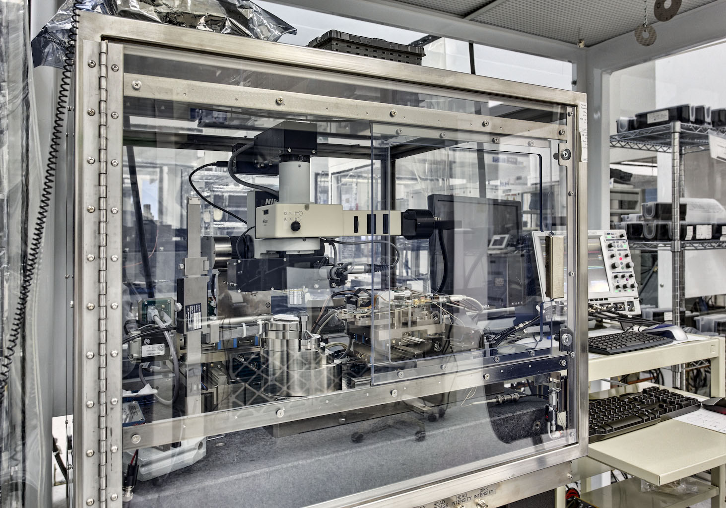
I know that part of my job is to make this tour fun and interesting for you, but sometimes we ran into barriers of multiple types. Take this photo of WD’s fly height test. As just mentioned, fly height is the distance between the magnetic head and the disk surface during a read/write operation. This is the machine that measures that distance. Given the lighting and angles and reflective enclosure surfaces, this was the best photo we were able to get. Maybe just use your imagination.
Other barriers proved to be more linguistic in nature. My generous engineer guide at this point explained the fly height test to me as follows. We both spoke English as a native language, although his dialect was clearly from Silicon Valley.
“[The] MicroPhysics Fly Height tester measures the spacing between the head and disk by using a rotating transparent replica of the magnetic disk together with an actual magnetic recording head with substantially improved accuracy at very low fly heights compared to the current industry standard methods. This fly height tester does not require a spacing varying calibration and does not make use of polarized light. The technique can be performed at substantially normal incidence to the Head/Disk interface and the precision of the spot location is not compromised as it can be on a non-normal incidence system.”
And moving on...
Gettin’ Even Hotter In Here
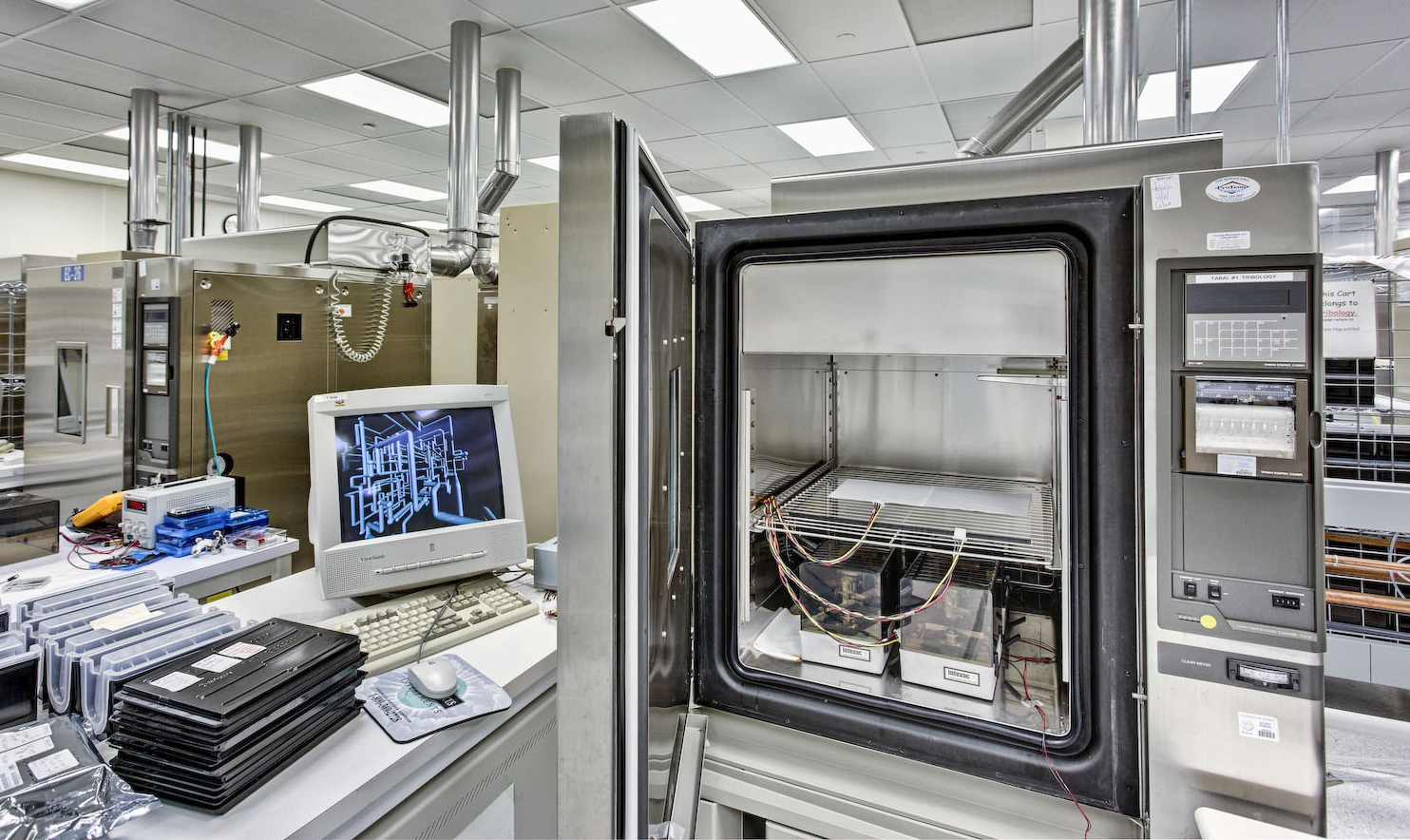
We all know that materials expand and contract as temperatures vary. So after WD finishes testing “flyability” under normal room conditions, they need to be stressed in order to determine the environmental range to which they can be pushed before failure. The oven you seen here is a Class 100 environmental chamber used to conduct head-media flyability tests under extreme temperature and humidity conditions. The chamber can be programmed to operate at a fixed condition—say, 90 degrees Fahrenheit at 20% humidity—or change conditions under programmed control. The stressed conditions are used to test for corrosion and accelerate failures so that engineers can identify any weaknesses in the media design. After all, the same drive you might use in the Alaskan winter also might wind up in an equatorial jungle. No drive can cover all extremes, but manufacturers have to be sure they cover at least 80% or 90% of common usage scenarios.
Get Tom's Hardware's best news and in-depth reviews, straight to your inbox.
Avoiding Friction
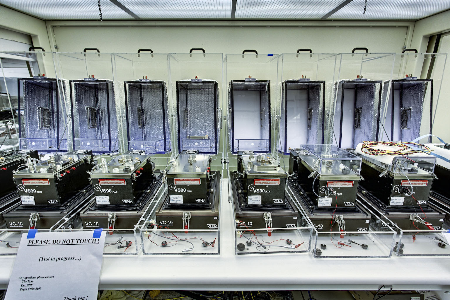
I confess, when we reached the disk testing systems, I thought we’d stumbled into a row of blenders in the employee lounge. Alas, drinks would have to wait. These machines measure head-media tribology. Tribology is the science of interacting surfaces in motion, a.k.a. friction. True, the head and media should never come into contact—again, that would constitute a head crash and wreck your drive—but the distance between them is so slight and the media is spinning at such high velocity that the air molecules between the head and platters can become a significant source of friction as they slam between the two solid objects. The tester is programmed to move the head across the disk, monitoring any interactions between the head and disk that could threaten reliability. It can also make a mean margarita with the right USB attachment. OK, no, it can’t.
A Real Tech Bench
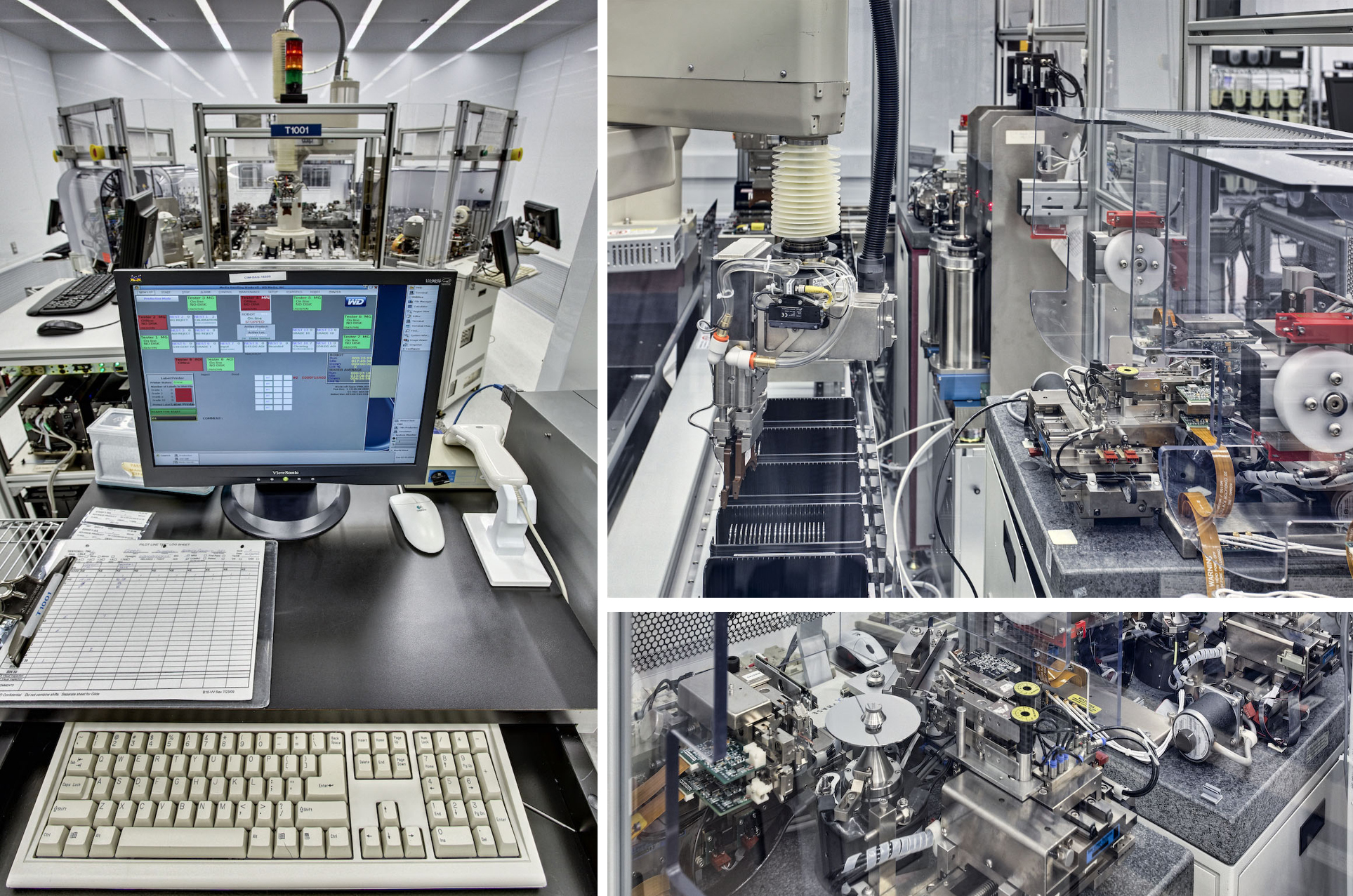
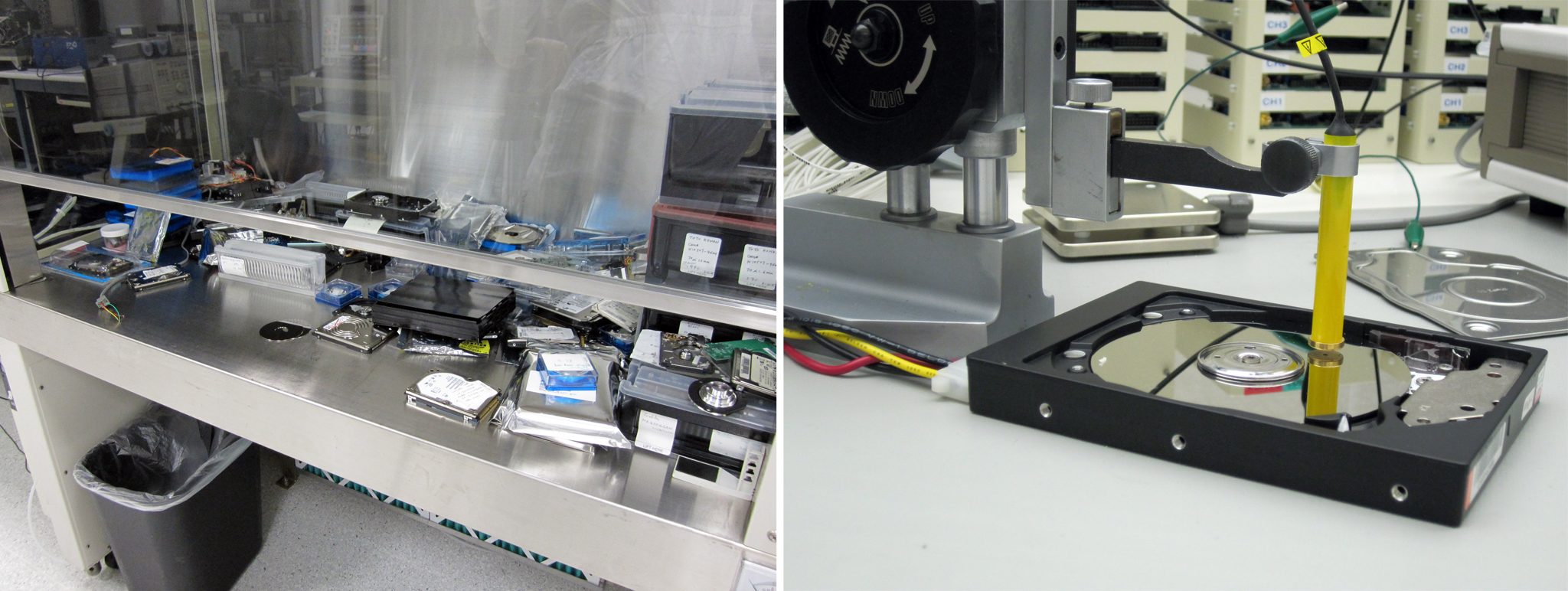
Inside the clean area, everything feels very odd and alien. The process of creating magnetic media requires very precise, stringent conditions. Eventually, though, the media has to go in an enclosure and be tested as an actual drive. Being “a drive” introduces a whole new set of component interactions and challenges. It’s the point where nano and micro go back to being macro. You’re back to being in the real world, and that’s when you see scenes like this: a real test bench, complete with piles and clutter and lots of little pieces everywhere. It might not be the image that WD would want to project to the world, but it’s reality, and the benchmarking geek in me felt just as interested in these benches as in the bizarre world of bunny suits. You don’t see six- and seven-figure machines dominating rooms here. This is where engineers tinker to work out the kinks and clicks. It may not involve much groundbreaking science, but it’s still important to the whole R&D process and ensuring a satisfactory end-user experience.
Analyze This
Forty percent of the San Jose 2 facility is dedicated to analysis. Despite the innocuous simplicity of a shiny little disk, there’s a substantial amount of examination and validation needed to confirm that each platter works as it should. Each disk has a sort of soft underlayer, then a couple of magnetic metal layers, then a carbon overcoat. Each layer may only be a few angstoms thick, and each needs to be analyzed for its individual characteristics.
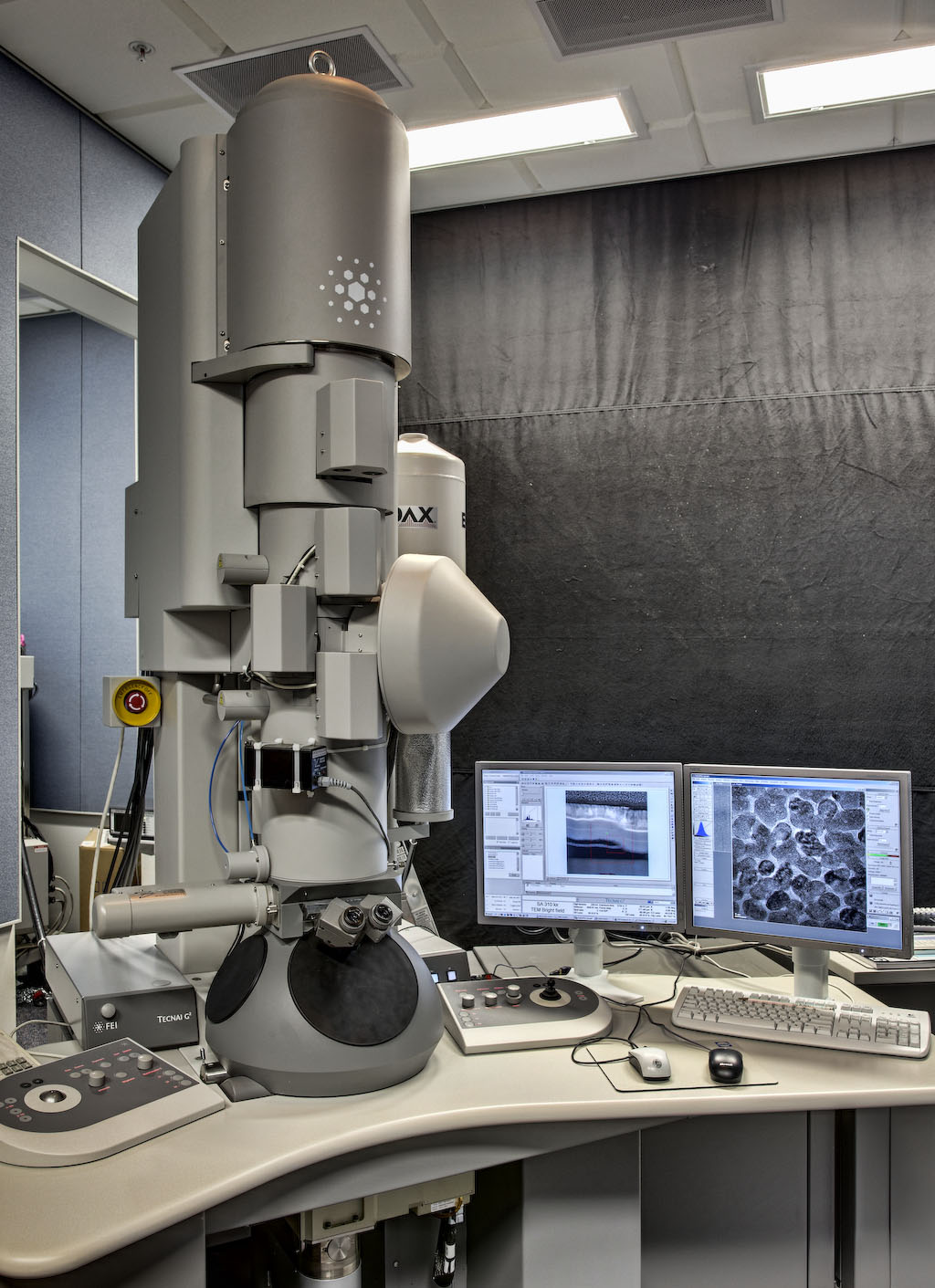
One machine for doing this is the Transmission Electron Microscope (TEM). When I approached this room, the door was closed and plastered with warnings, reminiscent of a studio recording chamber or a photography darkroom. After a few moments, the technician inside ushered us into a tiny space not much larger than the desk you see here. Modern TEMs can achieve magnifications of over 1 million times. In this setting, WD is using the TEM to examine media crystal structure, grain dimensions, and sputtered layer thickness. According to the technician who showed us this room, “it can also provide high-spatial resolution diffraction or chemical element analysis.”
Gaining Visibility
The TEM examines a disk sample, but each sample has to be specially cut in a circle by a instrument called the FIB, or Focused Ion Beam. The FIB takes the disk and remove a very small, thin slice from its back—so thin that about 1,000 slices would be as thick as a human hair. The sample gets placed on a specialized grid, and that grid then gets introduced into the TEM. An electron beam gets generated at the top of the column, shoots through the middle of the TEM column, and actually transfers through the sample. There are two ways to orient a sample in relation to the electron beam. You can either do it in “plane view,” perpendicular to the beam so you’re shooting from the sample’s top to its bottom, or in a cross section, so the beam shoots in one edge of the sample and out the opposite edge.
You probably recall from the recent shift to perpendicular magnetic recording that whereas magnetic grains used to lie flat on media, now they stand upright like grains of rice. But the composition, appearance, spacing, and so on of these grains is critical. The TEM will show you the difference it makes when grains are grown with, say, one degree of temperature variance from one process run to the next.
Peeling The Layers
Ideally, grains would all grow identically, but that simply doesn’t happen. As magnetic material gets deposited, the grain will orient based on the substrate material, and that orientation in turn influences how the grain develops, or “grows” as the WD engineers say. But grains can grow at different angles, the underlying lattice may shift, and many other seemingly random elements can influence the end result. A change in the sputtering process can seek to accentuate the size of the grain or modify its crystalography in a way that will enhance the disk’s magnetic performance, meaning its effective areal density.
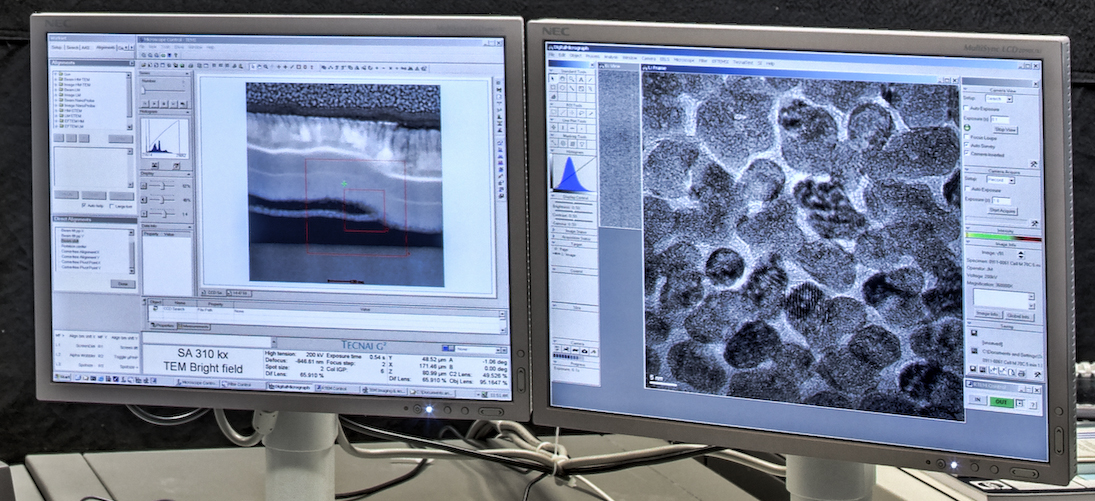
In this close-up, the left screen shows a cross-section with a defect (the dark area) under the thin film. The center area is called the soft underlayer, the material above that is the actual magnetic stack, and the topmost layer is protective coating.
“High magnification of images can also provide elemental information,” noted WD. “The process of the electron passing through the sample generates X-rays. So we can look at the energy of those X-rays and can get the elemental composition of each one of the layers. Once we determine the composition of a layer, we can decide if we want to increase one element over another. The process is also useful for failure analysis.”
Not Your Usual Dell XPS
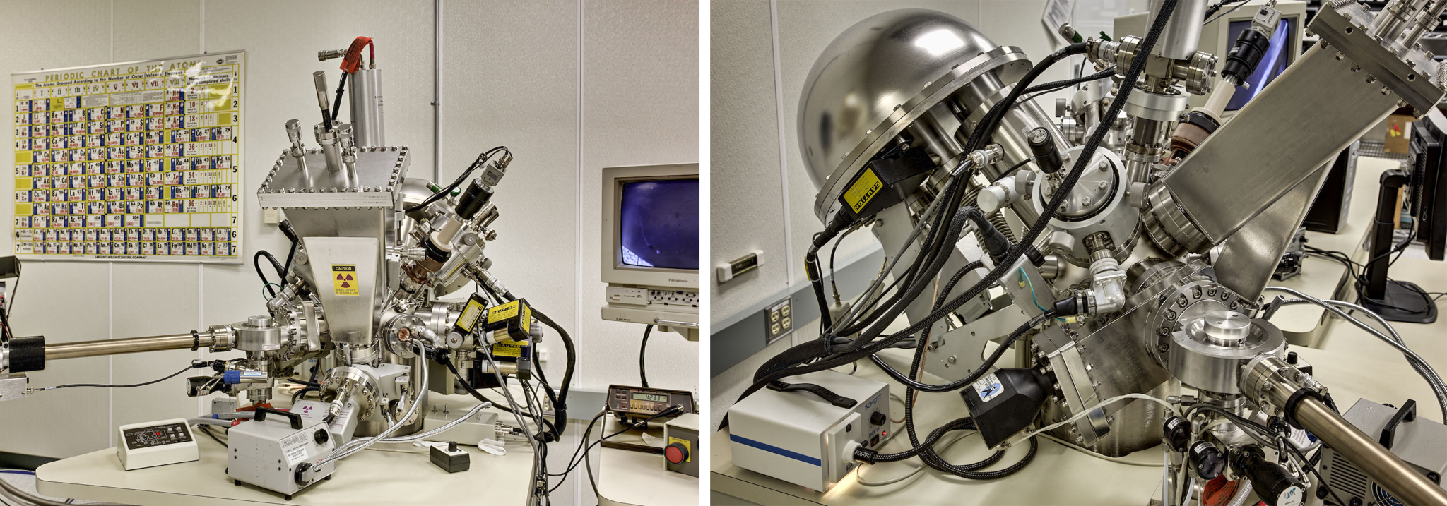
Analysis doesn’t begin or end with the TEM. I was shown two additional machines capable of equally powerful but very different types of materials analysis. Both were housed in a room that somehow reminded me very much of my high school science lab. Perhaps it was the periodic table poster on the wall, speckled linoleum tiling, and aesthetic love affair with gray and beige. In any case, the two machines before me looked like no instruments I’d ever seen before, a seemingly haphazard hodgepodge of gleaming columns, rivets, and tubing.
The first machine was a tool for ESCA (Electron Spectroscopy for Chemical Analysis; also known as X-ray Photoelectron Spectroscopy, or XPS). ESCA is used to determine surface atomic composition and chemical bonding. When a sample gets bombarded with aluminum K-alpha X-rays, it will emit electrons characteristic of the chemical elements present within a few nanometers of the surface.
“The electrons are separated by energy through the hemispheric analyzer,” explained the resident tech. “By analyzing the energy of those electrons, we can identify the element from which that electron came. By looking even closer at the energy of the electron, we can evaluate the chemical bonding states of that atom’s electron from the element it came from.”
We Could Tell You, But Then...
ESCA analyzes the top few hundred angstroms of a surface, so Western Digital uses it to examine the various sputtered layers within media. Specifically, WD uses ESCA to quantify surface lubricant and protective carbon layers under 2nm thick on disk media. This is critical to understanding the tribological performance of the head/media interface inside a drive.
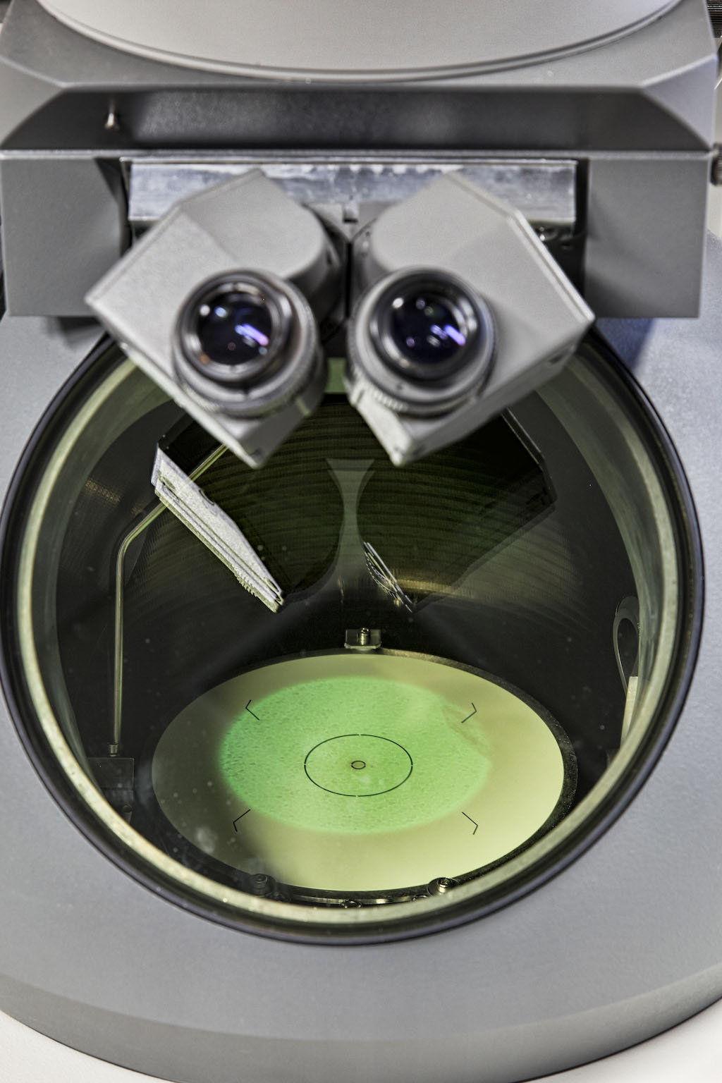
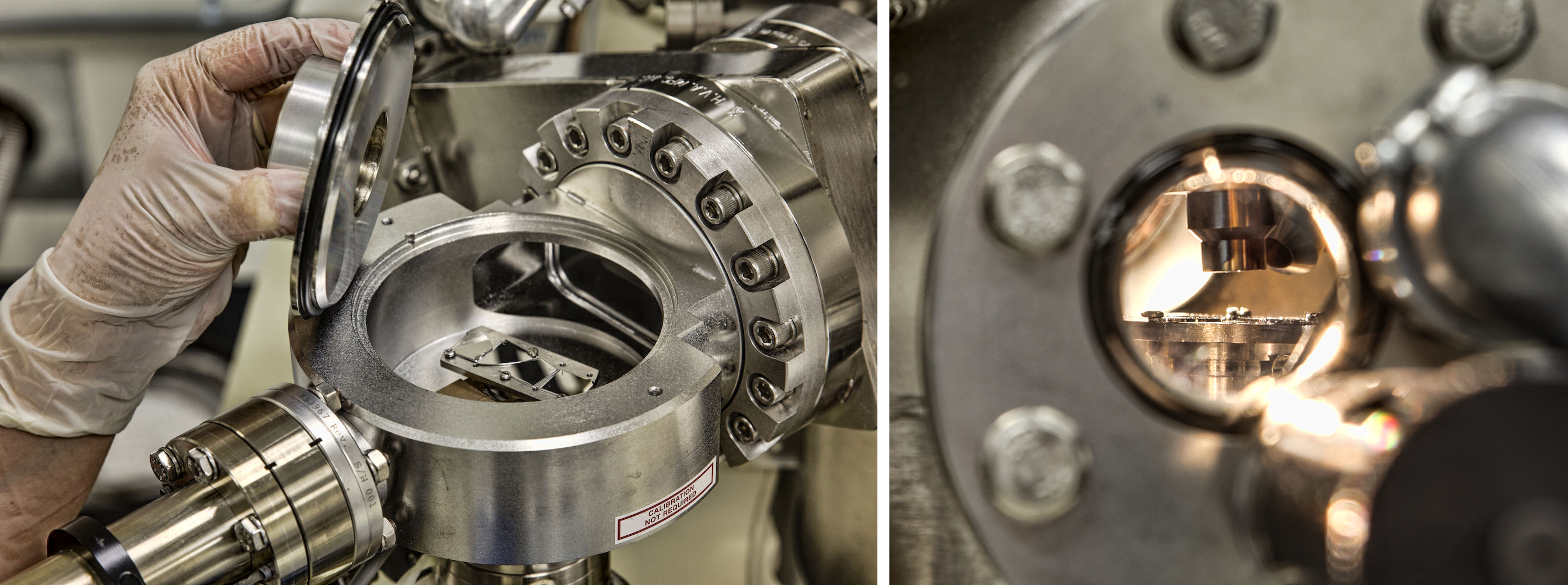
Technicians scribe little circles into disk media shards and load these into the ESCA tool to be analysis targets. These two pictures show the stage on which the shards sit, one view from the top and the other through a little peephole on the side.
“One thing we do is measure carbon thickness, and the exact thickness is specified by the given product,” noted our guide. “We have a thickness range of so many angstroms for each of the products. If it extends beyond a few angstroms out of range, they have to redo the process. The exact range is secret.”
-
zelog I'm guessing the metal plate on the floor in picture 29 is slightly elevated to let the water drain.Reply -
johnbilicki There are a lot of DOA complaints on Newegg and even with 40% of that place is required to make sure the drive works before it leaves the building it still has to go through shipping...UPS shows up eight hours after FedEx and the drive it dead because during shipping your package was the substitute baby for 'kick the baby'.Reply -
milosz It's amazing that all this precision work and exotic manufacturing technology can be had for $150Reply -
anamaniac Awesome. =DReply
I've switched to Samsung drives though. ^_^
And at the pic on page 26, she's checking her farmville. (At my job we hired an insanely expensive technician to fix some really expensive equipment, which he did with his laptop... and he has checking his farmville... at a few hundred dollars per hour on the company dime of course.)
Interesting that there appeared to be no drainage for the emergency shower. They just jerry rig that thing up at the last moment and hope no one has to use it?
Also, that walkthrough video is quite depressing. Yellow rooms as far as the eye can see, without a smile in sight.
Thank you very much for this wonderful article. As much as I'd like to, I doubt I could ever work there, because my handa aren't stable enough just to take a damned picture, nevermind handle extremely precise equipment. =)
But I wonder, how many drive failures have they had because an employee dropped a contact into the drive?
Also, great to see that little sneak preview on WD NAND based storage.
Now, how about Intel and 32nm? -
kikireeki And a new HDD is born and it is DOA! "sarcasm"Reply
I just hope that WDD has done it right this time! -
jhanschu I'm under the assumption that most of the pictures were taken in a "clean room" environment. As such, the floor grating would be elevated (as previously mentioned) for the laminar air flow and there may possibly be a drain below. Also if I noticed correctly, the ceiling "tiles" were actually HEPA filters.Reply -
g00ey I'm not buying that every step visualized on these photos are being applied to each and every platter that is manufactured on this facility. For example I don't think they examine the layers of every platter in the TEM. I believe the photos don't only show the manufacturing line but also some of the research facilities for next generation products.Reply
I think the manufacturing process is very much like an assembly line process where the production flow is rather fluent which is not the impression I get at a first glance when looking through these photos. They obviously achieve som degree of economies of scale. It would be interesting too see some figures such as how long it takes to produce a platter, head, and so on and how many units/components per hour that is being produced etc.
Then look at for example picture 28 (or 25-32); I don't understand how these large electoplated platters turn into read/write heads of a harddrive. I don't see the part where these wafers are punched into small needles (sliders/heads) and how this is done. -
neiroatopelcc I find it marvelous to see all this expensive hightech and amongst those things find old crt monitors and I think in one picture about #20 I even spotted an old hp dx2000 in the right side of an image (in front of an older 13" or so crt. Really nice to see expensive mashinery associated with expensive downtime being operated using windows antique and old hardware. Seems you don't always NEED a quadcore to be effective.Reply
Great article btw. Not sure I share the authors humor, but I suppose it beats kevins.
