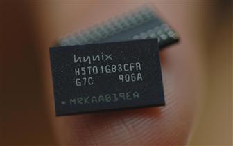
Hynix Produces 40nm 1 GB DDR3 for Q3'09
Get Tom's Hardware's best news and in-depth reviews, straight to your inbox.
You are now subscribed
Your newsletter sign-up was successful
Sunday South Korea's Hynix Semiconductor said that it has developed the world's highest-density memory chip built on 40nm process technology.
As technology progresses, sometimes bigger isn't always better. Case in point: Hynix Semiconductor has figured out how to develop 1 GB DDR3 DRAM (dynamic random access memory) built on 40nm process technology... in other words, the circuits within this new memory chip are just 40 nanometers apart. To put its size in perspective, a nanometer is one-billionth of a meter. As a result, the new chip is no larger than an adult fingernail.
Hynix's new DRAM will deliver a maximum speed of 2133Mbps and show a 50 percent productivity increase over the previous 50mn process technology, requiring less energy than its predecessor. The company also said that the new product will be cheaper to make, and by applying three-dimensional architecture, will see minimal leakage current.
"Hynix has become the world's first to apply the 40-nanometre-class technology to the DDR3 DRAM chip successfully," said Hynix spokesman Park Hyun. "The new chip development will help the company continue to lead the fast-changing memory chip market."
However, due to the plunging global economy, the memory chip industry has taken a huge hit below the belt. Still, the company hopes to expand its DDR3 specification and 40nm technology to other products including mobile DRAM, graphics DRAM, and even mass storage memory modules. That's bold news considering Toshiba slashed flash memory production at the beginning of the year, reducing output by 30 percent.
Hynix said that the new 40nm 1 Gb DDR3 is slated to enter mass production in Q3 2009.
Get Tom's Hardware's best news and in-depth reviews, straight to your inbox.

Kevin Parrish has over a decade of experience as a writer, editor, and product tester. His work focused on computer hardware, networking equipment, smartphones, tablets, gaming consoles, and other internet-connected devices. His work has appeared in Tom's Hardware, Tom's Guide, Maximum PC, Digital Trends, Android Authority, How-To Geek, Lifewire, and others.
-
lamorpa "taken a huge hit below the belt"?Reply
Maybe this would be more clear if you stated
"taken a huge hit below the belt, in the nuts, where it hurts a lot"
or
"taken a huge hit below the belt, in the nuts, where it hurts a lot, because that is a sensitive area"
-
Greatwalrus Yay! More technological advancements.Reply
I assume this won't be limited to just 1 Gb chips, right? -
computerninja7823 ok so now companies like Nvidia should go out get some of this and redo there GTX295...or just make sure the they put the correct amount of V-RAM on there new GTX 3** GX2's.., i mean common...look at the 9800GX2 it suffered from lack of V-RAM and so did the new GTX295....oh wellReply -
Sad Panda GreatWalrusI assume this won't be limited to just 1 Gb chips, right?Reply
1 Gb = 125MB, so the answer is no.
-
joebob2000 Reply...the circuits within this new memory chip are just 40 nanometers apart. To put its size in perspective, a nanometer is one-billionth of a meter.
That doesn't really put it in perspective, it performs some simple math. Perspective would be to say "a human hair is 2500 times wider than one of these transistors." -
sublifer hmmm... throughout the article you refer to it as 1GB chips then at the end you mention the 1Gb chips (which is more plausible) can you please correct the article to reflect the correct size?Reply
8Gb = 1GB -
ckthecerealkiller subliferhmmm... throughout the article you refer to it as 1GB chips then at the end you mention the 1Gb chips (which is more plausible) can you please correct the article to reflect the correct size? 8Gb = 1GBThey are 1Gb chips.Reply
