Cadence Design Systems and TSMC to Develop 16 nm FinFET Design Infrastructure
Cadence Design Systems and the Taiwan Semiconductor Manufacturing Company (TSMC) have launched a collaborative effort to develop 16 nm FinFET technology.
Cadence Design Systems and the Taiwan Semiconductor Manufacturing Company (TSMC) have entered into an ongoing multi-year agreement to develop the design infrastructure for 16 nm FinFET technology with a specific focus on "advanced node designs for mobile, networking, servers and FPGA applications." This deep collaborative effort is intended to effectively address the design challenges specific to this type of technology and hopes to deliver the requisite infrastructure for ultra low-power, high-performance processors.
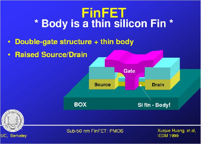
FinFETs are a form of multi-gate devices that were invented over a decade ago and distinguished by the conducting channel being wrapped by a thin silicon "fin" which forms the body of the device. This allows the production of transistors with low leakage currents and fast switching performance.
"The FinFET device requires greater accuracy, from analysis through signoff, and that is why TSMC is teaming with Cadence on this project," said Suk Lee, TSMC Senior Director, Design Infrastructure Marketing Division. "This collaboration will enable designers to use the new process technology with confidence earlier than ever before, allowing our mutual customers to meet their power, performance and time-to-market goals."
Article continues below"Producing the design infrastructure necessary for these types of complex, groundbreaking processes requires close collaboration between foundries and EDA technology innovators," said Chi-Ping Hsu, senior vice president, Silicon Realization Group at Cadence. "In joining with TSMC, a leader in FinFET technology, Cadence brings unique technology innovations and expertise that will provide designers with the FinFET design capabilities they need to bring high-performance, power-efficient products to market."
Get Tom's Hardware's best news and in-depth reviews, straight to your inbox.
Tarun Iyer was a contributor for Tom's Hardware who wrote news covering a wide range of technology topics, including processors, graphics cards, cooling systems, and computer peripherals. He also covered tech trends such as the development of adaptive all-in-one PCs.
-
ojas Haha somebody was saying something about TSMC moving to 16nm next year. If they're still in the design stage...i'm pretty sure its far off.Reply
