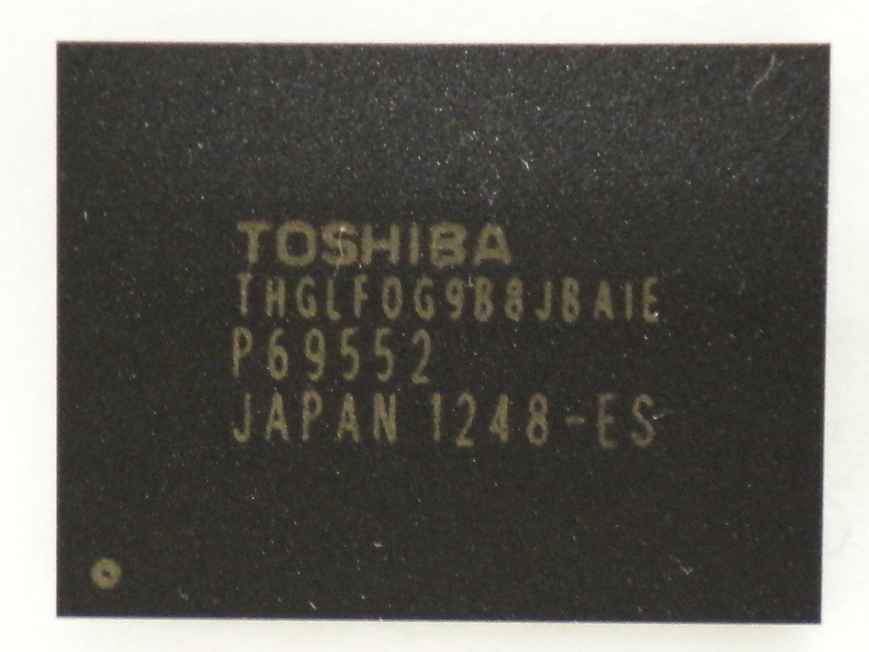
Toshiba Sampling 64GB UFS-Based NAND chips
Toshiba is now shipping 64 GB NAND flash modules using the UFS interface.
Get Tom's Hardware's best news and in-depth reviews, straight to your inbox.
You are now subscribed
Your newsletter sign-up was successful
Toshiba said last week that it began sampling out new 64 GB embedded NAND flash memory modules packed with a UFS interface (I/F). Designed for a wide range of small form factor products like smartphones and tablets, the new module is fully compliant with the JEDEC UFS v1.1 standard and supports the use of "lanes".
"The JEDEC UFS Ver.1.1 compliant interface handles essential functions, including writing block management, error correction and driver software," Toshiba said. "It simplifies system development, allowing manufacturers to minimize development costs and speed up time to market for new and upgraded products."
The company said the new modules are sealed in a small FBGA package measuring a mere 12- x 16- x 1.2-mm and uses 169 balls. Voltage ranges from 2.7V to 3.6V for the memory core, 1.7V to 1.95V for the controller core, and 1.10V to 1.30V for the UFS interface signals.
Article continues belowThe UFS serial interface has scalability the in number of lanes and speed. Toshiba's new modules offer single upstream and downstream lanes with 2.9 Gbit/sec bandwidth. Samples now shipping are mainly intended for evaluation of the UFS interface and its protocol in host chipsets and by OS vendors.
"Demand continues to grow for large density, high-performance chips that support high resolution video, driven by improved data-processing speeds in host chipsets and wider bandwidths for wireless connectivity," the company said. "Toshiba has proved itself an innovator in this key area, and is now reinforcing its leadership by being first in the industry to support samples with a 64GB UFS module."
Commercialization will depend on how receptive OEMs will be with these new chips using the UFS standard, so stay tuned.
Contact Us for News Tips, Corrections and Feedback
Get Tom's Hardware's best news and in-depth reviews, straight to your inbox.

Kevin Parrish has over a decade of experience as a writer, editor, and product tester. His work focused on computer hardware, networking equipment, smartphones, tablets, gaming consoles, and other internet-connected devices. His work has appeared in Tom's Hardware, Tom's Guide, Maximum PC, Digital Trends, Android Authority, How-To Geek, Lifewire, and others.
-
saturnus UFS, or in laymans terms USB gone SCSI, is a very interesting technology for mobile devices that could over time make actual separate volatile memory redundant as the transfer rates using only a single lane offer half the transfer rate as current LPDDR2 memory. One could easily imagine that with several lanes to each module and more modules in parallel could replace the need for DRAM in mobile devices altogether.Reply -
ojas saturnusUFS, or in laymans terms USB gone SCSI, is a very interesting technology for mobile devices that could over time make actual separate volatile memory redundant as the transfer rates using only a single lane offer half the transfer rate as current LPDDR2 memory. One could easily imagine that with several lanes to each module and more modules in parallel could replace the need for DRAM in mobile devices altogether.Give it 5 years and Intel will integrate this into their CPUs... :lol:Reply
But actually...if what you're saying is correct...it would be kind of cool, to have one of these as an expansion card to your mobile devices. Increase RAM and storage simultaneously. -
josejones The article discusses "64 GB embedded NAND flash memory modules" but doesn't explain what the previous specs were so, how are us noobs suppose to know what the upgrade really is when the article doesn't give us the last model specs to compare it to?Reply -
master_chen Reply
Those balls are still "small balls"...geddit?10435262 said:169 balls.........! Wow! That's a lot of balls for a tiny chip :D -
richwaa @saturnus: Sorry to disagree with you about UFS eventually making the need for separate volatile RAM redundant; it will not. UFS is an evolved interface spec for flash memory and does nothing to eliminate the inherent limitations in the flash memory itself. The number of memory operations that occur with code execution would create inherent instabilities in the current flash technologies that we don't know how to overcome --- yet. Running flash modules in parallel, as you suggest, would greatly exacerbate the already known problems with flash technologies; there's are really good reasons why disk/flash access moved from parallel to serial access such as clocking, capacitance, etc.Reply
http://en.wikipedia.org/wiki/Flash_memory#Limitations -
richwaa @saturnus: Sorry to disagree with you about UFS eventually making the need for separate volatile RAM redundant; it will not. UFS is an evolved interface spec for flash memory and does nothing to eliminate the inherent limitations in the flash memory itself. The number of memory operations that occur with code execution would create inherent instabilities in the current flash technologies that we don't know how to overcome --- yet. Running flash modules in parallel, as you suggest, would greatly exacerbate the already known problems with flash technologies; there's are really good reasons why disk/flash access moved from parallel to serial access such as clocking, capacitance, etc.Reply
http://en.wikipedia.org/wiki/Flash_memory#Limitations
