Intel takes final hurdle on way to mass-produced silicon laser chips
Santa Clara (CA) - Researchers at Intel and the University of California, Santa Barbara (UCSB) today said they have succeeded in building the world's first hybrid silicon laser using standard silicon manufacturing processes. The technology could be become a key enabler to make photonic interconnects in mainstream communications and computing devices a reality.
The new device announced today builds on an earlier announcement by Intel, which described an approach to use inexpensive silicon instead of pricey exotic materials as optical material and a foundation to amplify a light source. But other than the first CW silicon laser demonstrated in April of last year, the new version combines Indium Phosphide as light source with "the light-routing capabilities of silicon into a single hybrid chip," Intel said.
While Indium Phosphide laser can endure higher temperatures than the CW laser, Intel said that the new laser design is significant as it paves the may to low-cost mass-production. In fact, Mario Paniccia, director of Intel's Photonics Technology Lab, said that the hybrid chips can be built in one of Intel's standard CMOS fabs.
Photonics research has been publicly discussed by Intel as a future option to build chip interconnects at least since 2001. First technology announcements were made back in 2004 with the first 1 GHz unit in February and up to 10 Gb/s bandwidth in April. The company followed up in 2005 with a silicon laser last year and now believes that a chip in fact could integrate up to 100 lasers on one die and provide a bandwidth of possibly up to 100 Gb/s each. In Paniccia's vision, such chips would combine photonics and electronics and merge communications and computing one platform.
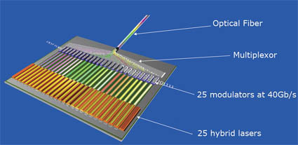
Basic principle of the photonics chip
The hybrid chip announced today used 36 lasers on one die that used 36 modulators and a multiplexor to route light beams with varying wavelengths through optical fiber. Each laser is about 1 micron wide and 800 microns long, which compares to the width of a human hair of about 100 microns. Down the road, Intel aims to combine the platform with a data receiver chip to build an integrated silicon photonic chip. The chip, currently considered part of Intel's "TeraScale" program to build processors with "10-100s" of cores, then would be built into computer boards and serve as interconnect between busses, between PCs and networks.
The actual performance capability of such devices are still to be seen, but Intel claims that 25 hybrid silicon lasers on a chip, would provide the aggregate bandwidth of 1 Terabit (25 x 40 Gb/s).
Get Tom's Hardware's best news and in-depth reviews, straight to your inbox.
Intel did not specify when such silicon laser chips would actually be available. However, with the claim that the "last major hurdle" is taken, Paniccia and his team appear to be well on track to meet an earlier announced goal and introduce the first photonic chips "by the end of the decade."
Tom's Hardware is the leading destination for hardcore computer enthusiasts. We cover everything from processors to 3D printers, single-board computers, SSDs and high-end gaming rigs, empowering readers to make the most of the tech they love, keep up on the latest developments and buy the right gear. Our staff has more than 100 years of combined experience covering news, solving tech problems and reviewing components and systems.


