Gigabyte Motherboard/Graphics Card Factory Tour
We take you through Gigabyte's production facility for a sneak peak of what goes on inside one of the world's leading motherboard and graphics card companies.
Secret Agent "Kobe"
This is THSA, or Tom's Hardware Secret Agent, codenamed Kobe. Thanks to her, we were able to get an inside look at what goes on at Gigabyte.
As many of you already know, Gigabyte is one of the leading manufacturers of computer components. Perhaps best known for its system boards and graphics cards, Gigabyte also manufactures servers, mobile phones, power supplies, coolers, and even networking products.
Today, however, we'll be taking a closer look at Gigabyte's motherboard and graphics card prodution facility. With Kobe being a component guru, she was the obvious choice at Tom's Hardware to do this undercover job.
Headquarters Made Of Heatsinks
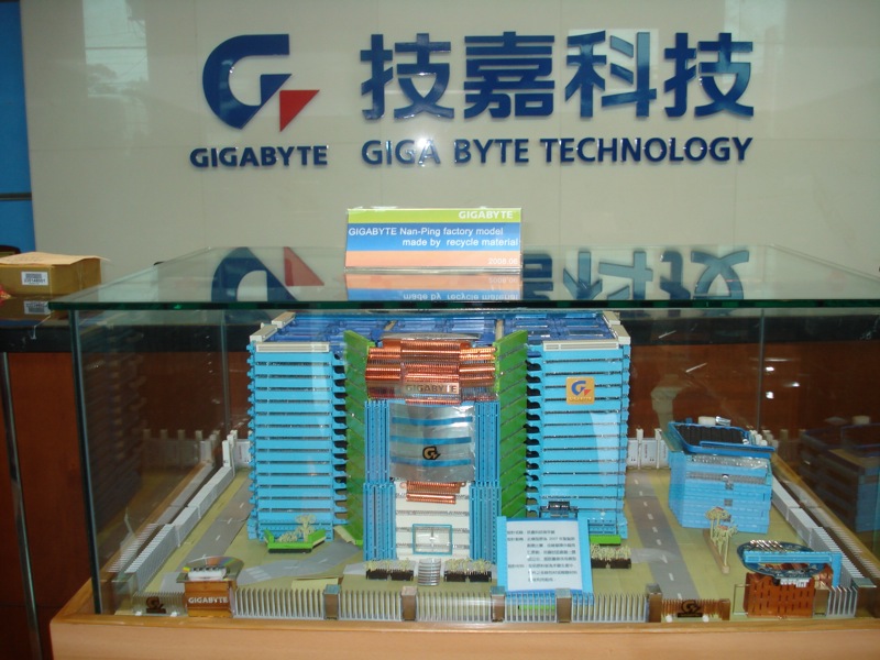
We start at the entrance, where Gigabyte has an actual model of its headquarters made from CPU trays, heatsinks, and other components that it sells.
The first step in motherboard design is figuring out what platform to design for. After this is decided, engineering teams work with chipset makers like AMD and Intel to come up with a product scheme. Once settled, reference designs are provided, and Gigabyte then goes through its initial work, defining actual board specifications and looking into possible third-party components to add value. Features like onboard RAID, sound, connectivity, and other extras are picked at this point.
Once the specs are finalized, the engineering team begins its layout job in software simulation. This allows for bug checking and other changes to be made before the layout goes to "the wire." During this process, engineers take everything into consideration--even the actual length of traces on a board.
Once done, layers are defined. Typically, you will see four-layer PCBs consisting of the following:
Get Tom's Hardware's best news and in-depth reviews, straight to your inbox.
Layer 1: Top layer. This layer carries signals
Layer 2: Copper. Power distribution
Layer 3: Copper. Ground
Layer 4: Bottom layer. Signaling
Signals can be passed through layers by what's known as a "via."
Components, routing, and layout are done on specialized layout software. Often times, several revisions are made to either tune, fix bugs, or change a component.
Of course, this is an oversimplification of the entire process, but this is essentially the major steps before a board enters production.
Where Things Are Made
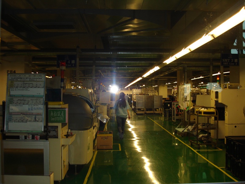
Above, we see the production facility.
Here the various components that will make up a finished product all gather. Everything from the PCB, resistors, sockets, chips, plugs, and brackets all come together in one harmonious process.
The manufacturing process is actually not entirely automated. There are steps in the process that require human intervention. Certain components are handled by technicians, but most of the work is performed by machines.
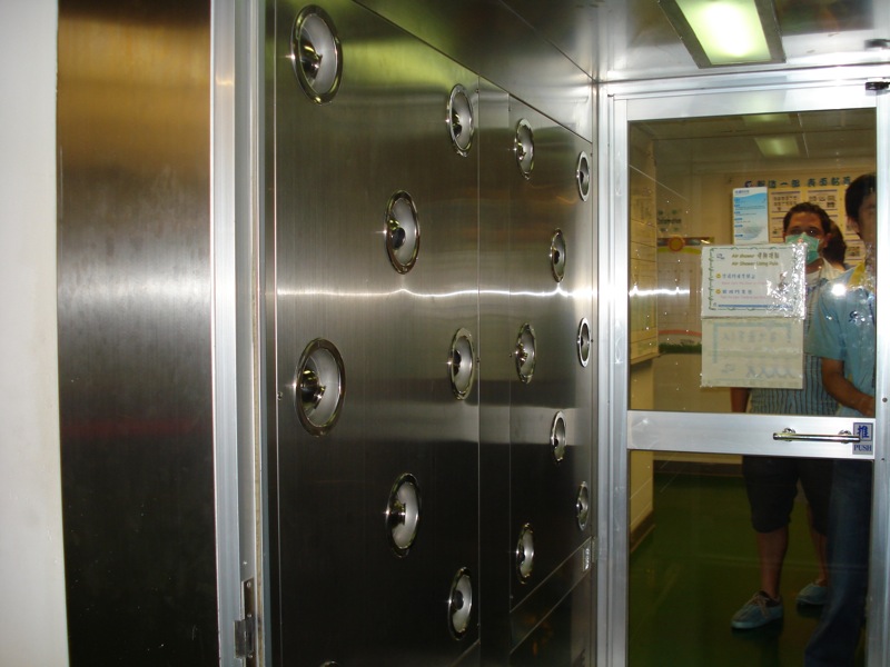
Before being allowed in the above area though, Kobe had to hop into a blast chamber to remove foreign particles from her clothes.
The Blast Chamber
A gust of air blasts you clean and particles are pulled upwards.
You come out of this room feeling Zestfully clean.
Above, you can see several people waiting to enter the blast room. They are wondering who the camera girl is.
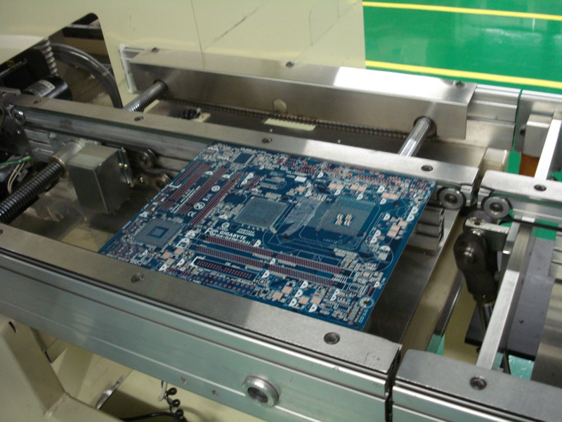
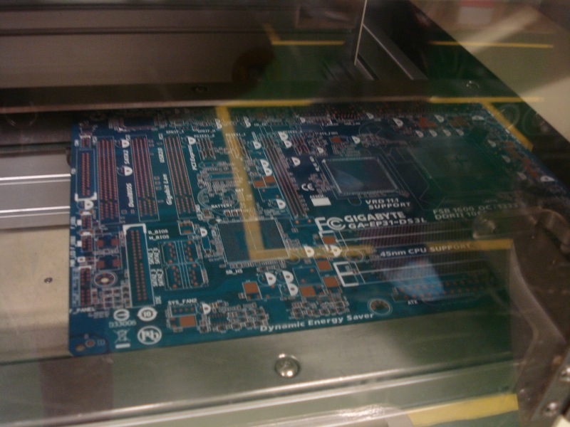
Blank PCB
Above, is a motherboard enjoying the ride through the production line, where it'll be populated with various components, and then eventually make its way over to the wave soldering machine.
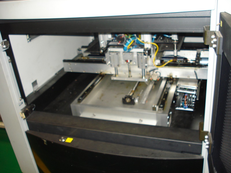
Through The Line
The board passes through several chambers, where various components are stacked.
SMT components are actually sent in on reels, like a film reel. This is where the term "tapped-out" comes from. Robots remove components from the reels and place them on the board with surgical precision.
Wave Soldering
Above, you can see part of a wave soldering machine.
The motherboard is covered with something called a solder mask, which seals the PCB from the liquid solder. The liquid solder immediately adheres to areas of the board where solder mask isn't applied--like connectors and soldering points. For top surface components, a process called reflow soldering melts solder paste that was pre-applied to the surface layer of the board. When the solder paste solidifies, the components are locked in place.
Quick factoid: solder mask is responsible for a board's color, which is typically green.
Click on the next slide for a YouTube video of wave soldering in action.
Wave Soldering, Again
Above, is a small wave soldering machine performing what's called selective wave soldering. Using this method, components can be selectively soldered onto a PCB.
This isn't the ideal method for large-scale production, used for smaller operations like board fixes.
A Bigger Wave
Above, is typically what a wave soldering line looks like.
Liquid solder flows in an arc, grazing the bottom of the PCB and adhereing to areas where the solder mask has not been applied.
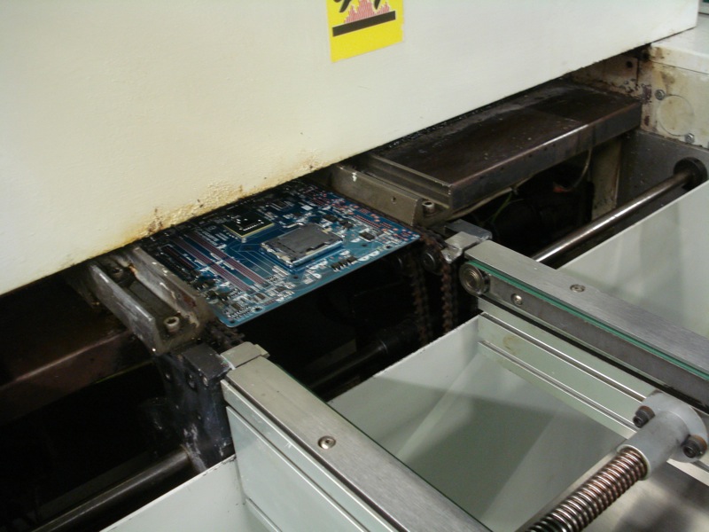
Out The Other End
A half-complete motherboard exists one wave soldering section, with the CPU socket and chipset attached.
The next phase is to solder on smaller components like resistors and capacitors. After this phase, the board will pass through a manual assembly line, where technicians populate the board with larger components like connectors and plugs.
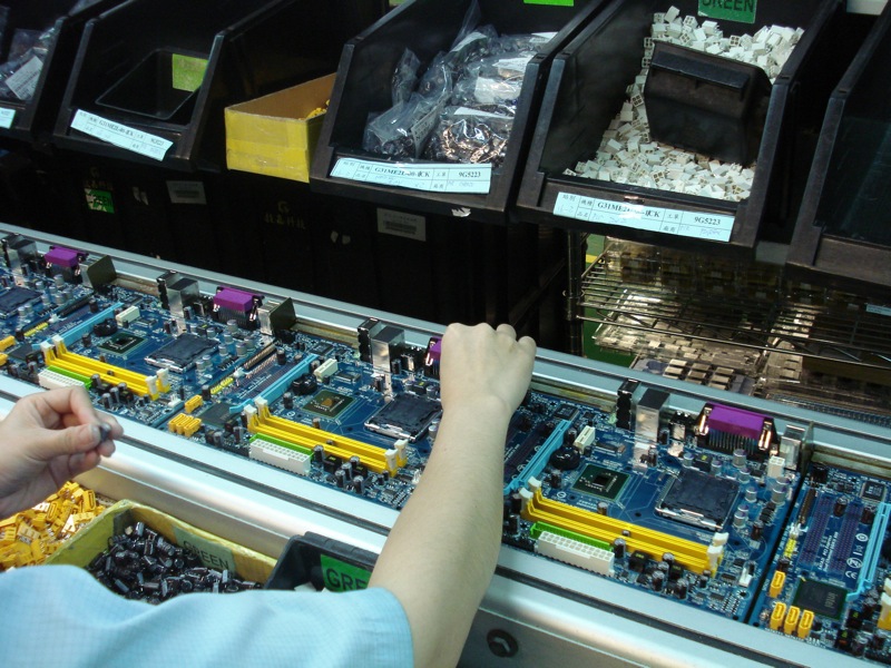
Nearly Hand-Built
Above, you can see a technician manually inserting a 12V CPU power jack.
-
08nwsula I heard if you are found sneaking around a Gigabyte plant they will cap your ass with 2 oz of copper.Reply -
computabug TH's comeback to business! Well, maybe not the same 'type' of business *cough* but at least it's getting readers back! :DReply -
computabug I thought that board was an HD4850, but it doesn't have the white DVI connectors... maybe they put it on last?Reply -
computabug Nevermind! I change my mind: it's a GTS250 for sure! Probably a 1gb OCed non-reference gts250Reply -
argade Correct me if I'm wrong but surface mount parts (SMT) come from tape and reel and are soldered in a reflow oven not a wave solder machine b/c they aren't through-hole parts. Also I believe flux is sprayed on the leads of the through-hole parts that need to be soldered in wave for a better solder joint, not the other way around.Reply -
computabug Ok sorry for 3 (almost) consecutive posts, but for picture 20:Reply
"With speed and skill, Sherri covertly moves in to bag a few motherboards and graphics cards."
Are you guys serious? T_T -
the last resort The video card in picture #14 is the 9800GT 1GB edition.Reply
http://www.newegg.com/Product/Product.aspx?Item=N82E16814125282
