ATI's Radeon X1950XTX: You Say You Want A RAM Revolution
Get Tom's Hardware's best news and in-depth reviews, straight to your inbox.
You are now subscribed
Your newsletter sign-up was successful
Meet The New Cards
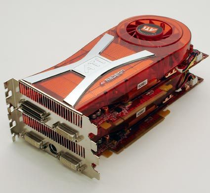
Radeon X1950 CrossFire Edition
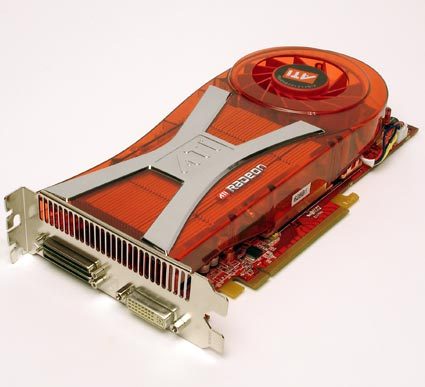
There are many cards that are being announced today. The flagship Radeon X1950XT and the Radeon X1950 CrossFire Edition both have a core clock speed of 650 MHz. This is a change from previous CrossFire Edition card specifications as they would generally be slower than the flagship card. This is good as the cards no longer will need to clock to a comparable speed or in other words, the XTX version will no longer have to go slower anymore.
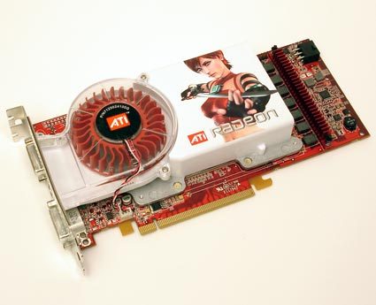
There are three other cards that ATI is announcing today as well: the Radeon X1900XT 256, the Radeon X1650 Pro and the X1300XT. The first card is the Radeon X1900XT 256, and it is equivalent in all regards to the previous flagship card Radeon X1900XTX except that it has 256 MB of GDDR3 memory instead of 512 MB. While there isn't a CrossFire-compatible card for the Radeon X1900XT 256, there is the strong possibility that it will later be able to double up in CrossFire mode via a software implementation.
The Radeon X1650 Pro is the identical card as the Radeon X1600XT, but with a new name and price. The same goes for the Radeon X1300XT, which formerly was the X1600 Pro. As with many new launches, the processors from previous generations find themselves on new boards with different names and credentials. In this case people are merely getting a price drop with a facelift.
We only received the Radeon X1950XTX, X1950 CrossFire Edition, and X1900XT 256 for testing. We are waiting on the Radeon X1650 Pro and X1300XT. The chart below shows the differences in the entire family. We will provide more coverage once we receive the additional cards.
| ATI Radeon X1950, X1900, X1800, & X1600 Specifications | ||||
|---|---|---|---|---|
| Row 0 - Cell 0 | X1950XTX | X1900XTX | X1900XT | X1900XT 256 |
| Process Technology | 90nm | 90nm | 90nm | 90nm |
| Number of Transistors | 384M | 384M | 384M | 384M |
| Core Clocks (Vertex, Core) in MHz | 650/650 | 650/650 | 625/625 | 625/625 |
| Memory Clock (MHz / data rate) | 1000/2000 | 775/1550 | 725/1450 | 725/1450 |
| Vertex Shaders (#) | 8 | 8 | 8 | 8 |
| Pixel Shaders (#) | 48 | 48 | 48 | 48 |
| ROPs (#) | 16 | 16 | 16 | 16 |
| Texture units | 16 | 16 | 16 | 16 |
| Frame Buffer Size | 512 MB | 512 MB | 512 MB | 256 MB |
| Memory Bandwidth (GB/sec) | 64 | 49.6 | 46.4 | 46.4 |
| Vertices/Second (Millions) | 1300 | 1300 | 1250 | 1250 |
| Pixel Fill Rate (# ROPs x clk) in Billions/sec | 10.4 | 10.4 | 7.2 | 7.2 |
| Texture Fill Rate (# Texture units x clk) in Billions/sec | 41.6 | 41.6 | 40 | 40 |
| RAMDACs | 400 MHz | 400 MHz | 400 MHz | 400 MHz |
| Bus Technology | PCI Express | PCI Express | PCI Express | PCI Express |
| Row 16 - Cell 0 | X1800XT | X1800GTO | X1600XT | Row 16 - Cell 4 |
| Process Technology | 90nm | 90nm | 90nm | Row 17 - Cell 4 |
| Number of Transistors | 321M | 321M | 157M | Row 18 - Cell 4 |
| Core Clocks (Vertex, Core) in MHz | 625/625 | 470/430 | 440/400 | Row 19 - Cell 4 |
| Memory Clock (MHz / data rate) | 750/1500 | 500/1000 | 690/1380 | Row 20 - Cell 4 |
| Vertex Shaders (#) | 8 | 8 | 8 | Row 21 - Cell 4 |
| Pixel Shaders (#) | 16 | 12 | 12 | Row 22 - Cell 4 |
| ROPs (#) | 16 | 16 | 16 | Row 23 - Cell 4 |
| Texture units | 16 | 16 | 4 | Row 24 - Cell 4 |
| Frame Buffer Size | 512 MB | 256 MB | 256 MB | Row 25 - Cell 4 |
| Memory Bandwidth (GB/sec) | 48 | 32 | 44.16 | Row 26 - Cell 4 |
| Vertices/Second (Millions) | 1300 | 940 | 880 | Row 27 - Cell 4 |
| Pixel Fill Rate (# ROPs x clk) in Billions/sec | 8.8 | 6.88 | 6.4 | Row 28 - Cell 4 |
| Texture Fill Rate (# Texture units x clk) in Billions/sec | 10 | 7.52 | 28.16 | Row 29 - Cell 4 |
| RAMDACs | 400 MHz | 400 MHz | 400 MHz | Row 30 - Cell 4 |
| Bus Technology | PCI Express | PCI Express | PCI Express | Row 31 - Cell 4 |
| NVIDIA GeForce 7950, 7900, 7800, & 7600 Specifications | ||||
|---|---|---|---|---|
| Row 0 - Cell 0 | 7950GX2 | 7900GTX | 7900GT | 7800GTX 512 |
| Process Technology | 90nm | 90nm | 90nm | 110nm |
| Number of Transistors | 556M | 278M | 278M | 302M |
| Core Clocks (Vertex, Core) in MHz | 500/500 | 700/650 | 470/450 | 550/550 |
| Memory Clock (MHz / data rate) | 600/1200 | 800/1600 | 660/1320 | 850/1700 |
| Vertex Shaders (#) | 16 | 8 | 8 | 8 |
| Pixel Shaders (#) | 48 | 24 | 24 | 24 |
| ROPs (#) | 32 | 16 | 16 | 16 |
| Memory Interface | 256-bit | 256-bit | 256-bit | 256-bit |
| Frame Buffer Size | 1 GB | 512 MB | 256 MB | 512 MB |
| Memory Bandwidth (GB/sec) | 76.8 | 51.2 | 42.2 | 54.4 |
| Vertices/Second (Millions) | 2000 | 1400 | 940 | 1100 |
| Pixel Fill Rate (# ROPs x clk) in Billions/sec | 16 | 10.4 | 7.2 | 8.8 |
| Texture Fill Rate (# pixel pipes x clk) in Billions/sec | 24 | 15.6 | 10.8 | 13.2 |
| RAMDACs | 400 MHz | 400 MHz | 400 MHz | 400 MHz |
| Bus Technology | PCI Express | PCI Express | PCI Express | PCI Express |
| Row 16 - Cell 0 | 7800GTX | 7800GT | 7800GS AGP | 7600GT |
| Process Technology | 110nm | 110nm | 110nm | 90nm |
| Number of Transistors | 302M | 302M | 302M | 178M |
| Core Clocks (Vertex, Core) in MHz | 470/430 | 440/400 | 375/375 | 560/560 |
| Memory Clock (MHz / data rate) | 600/1200 | 500/1000 | 600/1200 | 700/1400 |
| Vertex Shaders (#) | 8 | 7 | 6 | 5 |
| Pixel Shaders (#) | 24 | 20 | 16 | 12 |
| ROPs (#) | 16 | 16 | 8 | 8 |
| Memory Interface | 256-bit | 256-bit | 256-bit | 128-bit |
| Frame Buffer Size | 256 MB | 256 MB | 256 MB | 256 MB |
| Memory Bandwidth (GB/sec) | 38.4 | 32 | 38.4 | 22.4 |
| Vertices/Second (Millions) | 940 | 770 | 562.5 | 700 |
| Pixel Fill Rate (# ROPs x clk) in Billions/sec | 6.88 | 6.4 | 3 | 4.48 |
| Texture Fill Rate (# pixel pipes x clk) in Billions/sec | 10.32 | 8 | 6 | 6.72 |
| RAMDACs | 400 MHz | 400 MHz | 400 MHz | 400 MHz |
| Bus Technology | PCI Express | PCI Express | AGP 8X | PCI Express |
While the technical launch is today, cards will not hit the shelves until September 14. Public relations manager Will Willis stated that "Card orders can be taken on August 23 but they won't ship until September 14." So if you want one you will have to wait but you can place your order today.
Get Tom's Hardware's best news and in-depth reviews, straight to your inbox.


