The 'GMCH' And Its Buses
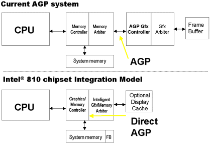
The 82810-chip is called 'GMCH', which stands for 'Graphics & Memory Controller Hub' . The name already says it, this chip includes the memory controller and the 2D/3D graphics engine of the 810-chipset. The GMCH has three external buses and one interesting internal bus, the above picture shows unfortunately only two external ones.
- The Memory Bus - 100 MHz, 64 bit = 800 MB/s
Surprisingly, Intel is running the memory bus at 100 MHz in 810, although the CPU-bus is only 66 MHz for now. This means that 810-boards will require PC100 memory, even though you plug in only a 66 MHz CPU. The memory bus is pretty straight forward, 64 bits wide, clocked at 100 MHz, thus offering a bandwidth of 800 MB/s, which is 50% more than the CPU bus bandwidth of only 533 MB/s. I guess this is the first time in PC-history, that the memory runs at a faster bus than the CPU, but who shall ever understand the logic of mighty Intel? A CPU is using an internal L2-cache clocked at processor clock and thus up to 466 MHz, to buffer the slow external bus of only 66 MHz, whilst the memory could deliver data faster at 100 MHz if this 66 MHz slow motion street wasn't in between them.
- The 'Interlink' Bus between GMCH and ICH - 133 MHz, 2x, 8 bit = 266 MB/s
We talked about it already, the graphics & memory controller hub is connected to the 'ICH' = 'I/O Controller Hub' using a special bus that offers 266 MB/s bandwidth, which is pretty cool and fast.
- The Internal 'Direct AGP' - 100 MHz, 64 bit = 800 MB/s
You can imagine it quite well, the 810-chipset doesn't come with an external AGP-connector, since its graphics controller is within the chipset already. Now it's no real big deal for the graphics controller to use textures from main memory or receive geometry data from the CPU, since it is on the same chip as the memory controller. Thus it can talk to main memory at the full 800 MB/s, which is faster than the 533 MB/s of AGP 2x. However, we shouldn't forget that the frame buffer of the 810-graphics is also found inside the main memory, and here the 800 MB/s look pretty pathetic compared to 3,200 MB/s and more local memory bandwidth, found on today's 3D accelerator cards.
- The Display Cache Bus - 100 MHz, 32 bit = 400 MB/s
The 810 can be equipped with an optional display cache of 4 MB. This cache is only supposed to be used in 3D-applications for the Z-buffer. Now I am seriously wondering why this bus comes with a bandwidth of only 400 MB/s. The Z-buffer of a normal 3D-card is residing within its local memory and thus accessible at 3.2 GB/s and above. 400 MB/s is even less than the main memory bandwidth, so that I wonder why 810 is supposed to run faster 3D-graphics when using external display cache at 400 MB/s, instead of using a Z-buffer from inside main memory at a peak bandwidth of 800 MB/s without display cache.
TOPICS