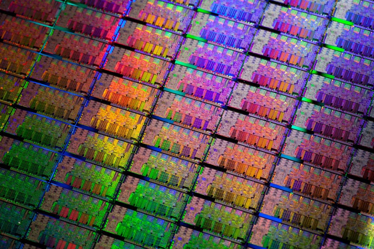
Intel's New Factory to Make 450mm Chip Wafers
Mmm, big crispy wafers.
Intel is building a new fab facility in Hillsboro, Oregon to handle 450mm wafers. According to the EETimes, the chipmaker is also going to upgrade current U.S. facilities for 22-nm production at a total investment of between $6 billion and $8 billion.
The new fab in Oregon will be known as D1X and will begin its R&D in 2013.
"Intel is very interested in 450mm… D1X is being (constructed) to be compatible with 450mm," said Intel's director of process architecture and integration, Mark Bohr, adding that equipment vendors are now interested in making 450mm tools.
Larger wafers mean that there will be a greater number of chips produced per cycle, which generally means a reduced cost on the producer that translates to lower prices for the consumer. (The same sort of principle occurs during a process shrink, where more chips can fit on a single wafer.)
Get Tom's Hardware's best news and in-depth reviews, straight to your inbox.
-
alidan dEAne22nm is very small, wonder how powerful devices at that time.well right now we have 45nm with 8 cores, expect 22 to have around 16, or possibly more l1,2,3 cashes or current 6 core and 12 logicals to be about half price (possibly between 1/3 and 1/2)Reply
what i want to know is what 450mm is. is it bigger than what they are currently using -
James296 @alidan think of the 22nm chip as a piece of paper and the 450mm as a gaint roll (of paper), that the piece of paper comes fromReply
P.S. this is just a simple way of viewing it -
agnickolov Current production uses 300mm wafers, so yes - it's definitely bigger, 2.25 times bigger in fact (1.5 times the diameter squared)Reply -
alidan James296@alidan think of the 22nm chip as a piece of paper and the 450mm as a gaint roll (of paper), that the piece of paper comes fromP.S. this is just a simple way of viewing itReply
i know that, but this quote here "Intel is very interested in 450mm"
meaning they aren't currently doing it, or atleast thats what it seams, what i want to know is if that means its bigger or smaller than whatever they currently use. -
Vilekon They are using smaller wafer sizes currently, I think around 300mm is the current size of wafers.Reply -
x4dm alidani know that, but this quote here "Intel is very interested in 450mm"meaning they aren't currently doing it, or atleast thats what it seams, what i want to know is if that means its bigger or smaller than whatever they currently use.wow, you really have no clue, do you?Reply

