

One of the highlights of Intel's first-quarter earnings report last week was improved sales of its client and data center processors as a result of improved output and yield, as well as high demand. Last week, industry analyst Ben Bajarin said the company was now selling what would normally be 'scrap' or 'low-expectation' CPUs, which helped boost margins. We followed up with industry veteran Dan Hutcheson for more details, and he notes that some of the company's recent yield gains are less about breakthrough inventions and more about disciplined execution improvements under its new manufacturing leadership.
Dan Hutcheson, vice chair of TechInsights, told Tom's Hardware that while techniques like binning and statistical process control (SPC) have been standard practice at Intel for about 40 years, recently — starting from around late 2024 when Naga Chandrasekaran, the current head of Intel Foundry, joined the company — Intel focused on tightening yield distribution across the wafer by reducing edge-related variability.
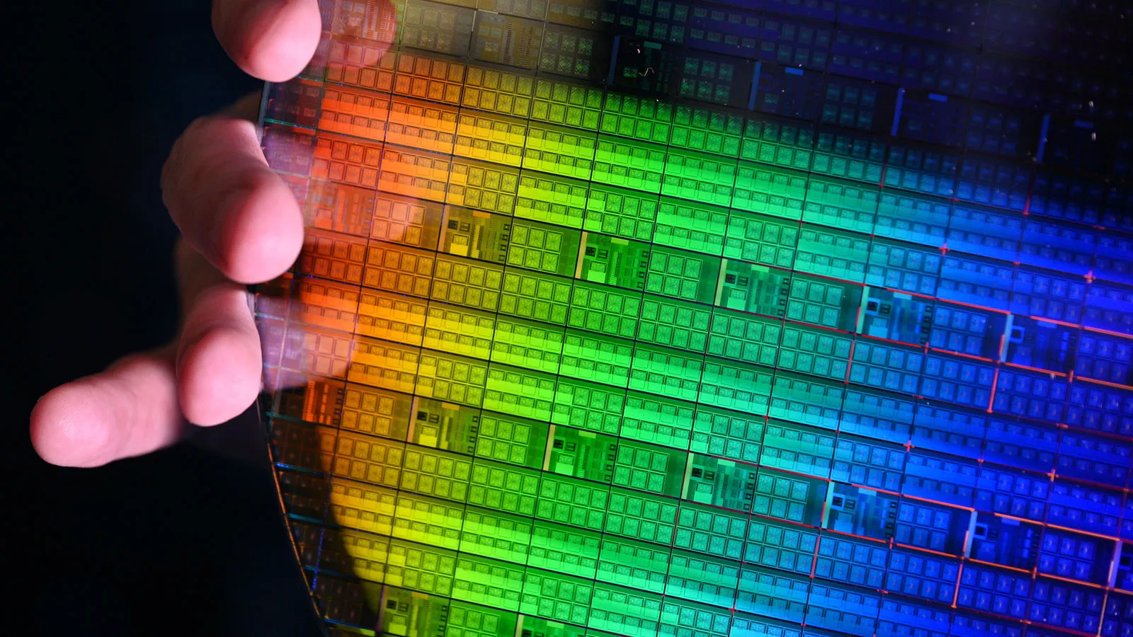
Specifically, Intel now runs a continuous process improvement (CPI) program after a node enters high-volume manufacturing, so by now it has implemented certain edge-specific process correction methods in a bid to reduce quality variability from the center to the edge of a wafer to get more sellable silicon from a single wafer.

"When it comes to manufacturing, it takes a year or two to make these kind of dramatic changes," Hutcheson told Tom's Hardware. "There’s just nothing new here. Intel has binned lots since the 1980s. Yield distributions are always heteroscedastic from the center to the edge of the wafer. Actually, one of the things Naga Chandrasekaran's yield management efforts have changed is to narrow the spread to the edge of the wafer. Hence, they are getting more revenue-per-wafer for little cost. The beauty of it is that the improvements are node independent."
As a result, Intel can now extract more high-quality dies from a single wafer and, perhaps even more importantly, more sellable dies from a single wafer, which improves output and productivity. Essentially, chips that previously might have been scrapped or too marginal to sell are now binned into lower-tier SKUs and sold because the demand is strong, according to Ben Bajarin, chief executive and principal analyst at Creative Strategies.
"Got some clarity from Intel IR on additional lift to margins," Bajarin wrote in an X post. "Intel got an unexpected margin lift from better yield salvage. Chips that would normally have been lower-value edge-die on the wafer were binned down and still sold into usable SKUs, turning what may have been scrap or low-expectation output into incremental revenue. Customers did not care, just said 'I will take it all.' That is the demand environment we are in for CPUs."
This can be interpreted in different ways, but it is feasible that the yield distribution improvements have made lower-quality chips now viable products, or that the company created even lower-tier SKUs to harvest even more chips.
More importantly, the aforementioned tightening yield distribution improvements are said to be largely node-independent, which means they benefit multiple process technologies rather than the existing nodes, such as Intel 7/4/3. Indeed, there are many ways to reduce edge-related variability, and many of them are node independent, which means some of the methods developed at Intel should be applicable to 18A (though that isn't confirmed). In fact, one of the comments Intel made during its earnings call is that the yield curve of 18A progresses at a pace that is higher than expected.
"Lip-Bu had a [18A yield] target as we came into this year for the end of this year, and we are probably going to hit that probably the middle of this year," said David Zinsner, chief financial officer of Intel. "So, you know, he has done a very good job working the team to drive a better response there."

Follow Tom's Hardware on Google News, or add us as a preferred source, to get our latest news, analysis, & reviews in your feeds.