Overview
Matrox describes Parhelia as the first 512-bit GPU (Graphics Processing Unit) in the world, which accounts for the "512" that appears in the full name for the chip. It comes with a 256-bit wide memory bus, which is able to transfer 512 bits of data per clock, because of its double data rate capability. This may just be a number to you, but in practice, this is some rather amazing stuff. It increases the pin count of the chip by an incredible number and it makes the PCB of the graphics card a lot more complex too. There's a good reason why neither NVIDIA, nor ATi have tried that yet. Right now, Parhelia demo boards have no less than 8 layers! At 300 MHz memory clock (600 MHz DDR), Parhelia has a whopping memory bandwidth of 20 GB per second. By comparison, NVIDIA's top product, the GeForce 4 Ti4600, just reaches 10.4 GB/s. However, with its Lightspeed Memory Architecture II, NVIDIA has provided its graphics cards with a very effective Crossbar Memory Controller, lossless Z-compression and further optimizations.
Parhelia also has an intelligent memory controller with several independent sub-controllers, which optimize the access of the intensity, depth, fragment and texture buffers. Furthermore, Matrox has implemented a fast Z Clear function. Various internal caches are designed to prevent bottlenecks in dataflow. Parhelia's units for depth, fragment AA, pixel, texture and display are each connected separately to the 512-bit memory controller array, and they also have a special function that optimizes memory throughput. The requests from these units are handled by the memory controller array. The array contains several independent controllers that simultaneously process various data.
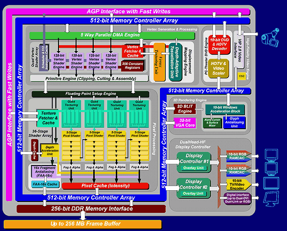
Matrox has tried to make the data throughput in the chip very efficient. For example, the texture fetcher and the cache are supposed to ensure maximum efficiency when reading texels from the textures in single-pass quad texturing and anisotropic filtering. Here, the texture fetcher calculates where a texel should come from, how many texels should be used and when, so that bottlenecks can be avoided. In addition, the memory is accessed as efficiently as possible during the process. The data are then stored in the texture cache and stand ready for the quad-texturing units.
Other interesting optimizations are related to the depth acceleration and the depth cache, which optimize access to the Z-buffer data. They also contain circuits for fast Z-clear functions, as well as sophisticated logic that combines the Z-reads and Z-writes so that they can be processed in burst access. As for the new AGP 8x interface, it remains to be seen whether this will offer a performance advantage in the future.
With regard to 3D features, the Parhelia-512 is positioned between DirectX 8.1 and the next version, DirectX 9. The quad vertex shader (v2.0) corresponds to DirectX 9, whereas the pixel shader still follows DirectX 8.1 version 1.3, as used by NVIDIA in its GeForce 4. At first glance, this is an odd combination, since vertex shaders can be emulated by the driver, while the emulation of pixel shaders can only be achieved with extreme loss of speed. Matrox argues that this is exactly why a modern vertex shader unit is worth it in practice. Game developers can use vertex shaders via emulation, without fearing that the functions won't work with end users. Therefore, it can be expected that the the newest versions of shaders will always be used in games. With pixel shaders, however, the developers have to be more careful because the latest versions of these functions can only run on a few cards. Pixel shaders from v1.3 and up will be most widespread among games, and in the future, they will become somewhat of a standard. However, it wouldn't hurt for Parhelia-512 to have a pixel shader unit based on DirectX 9, either.