Intel’s Second-Gen Core CPUs: The Sandy Bridge Review
Although the processing cores in Intel’s Sandy Bridge architecture are decidedly similar to Nehalem, the integration of on-die graphics and a ring bus improves performance for mainstream users. Intel’s Quick Sync is this design’s secret weapon, though.
Inside Of Sandy Bridge: Cores And Cache
From 10 000 feet, the Sandy Bridge die you saw on the previous page looks like a complete departure from its predecessor. After all, the mainstream Clarkdale-based CPUs consisted of two physical chips—a dual-core CPU manufactured at 32 nm and a graphics core/integrated memory controller/PCI Express controller etched at 45 nm. Now we’re looking at a single 32 nm part with all of those capabilities crammed onto one piece of silicon. Drill down, though, and there are really a lot of similarities that turn out to be more evolutionary in nature.
For each piece of Sandy Bridge that you look at, keep one word in mind: integration. Intel wanted to get the most out of each of the architecture’s nearly 1 billion transistors (the official count is 995 million).
There are actually three different versions of the Sandy Bridge die shipping at launch. The quad-core configuration—the one composed of 995 million transistors—measures 216 mm². Then, there’s a dual-core die with 12 execution units making up its graphics engine. That one features 624 million transistors on a 149 mm² die. Finally, the slimmest variation sports two cores and a graphics engine composed of six EUs. Though it’s flush with 504 million transistors, you’d hardly know it given the 131 mm² die size.
| Header Cell - Column 0 | Die Size (square mm) | Transistors (million) |
|---|---|---|
| Sandy Bridge (4C) | 216 | 995 |
| Sandy Bridge (2C, HD Graphics 3000) | 149 | 624 |
| Sandy Bridge (2C, HD Graphics 2000) | 131 | 504 |
| Bloomfield (4C) | 263 | 731 |
| Lynnfield (4C) | 296 | 774 |
| Westmere (2C) | 81 | 383 |
| Gulftown (6C) | 248 | 1168 |
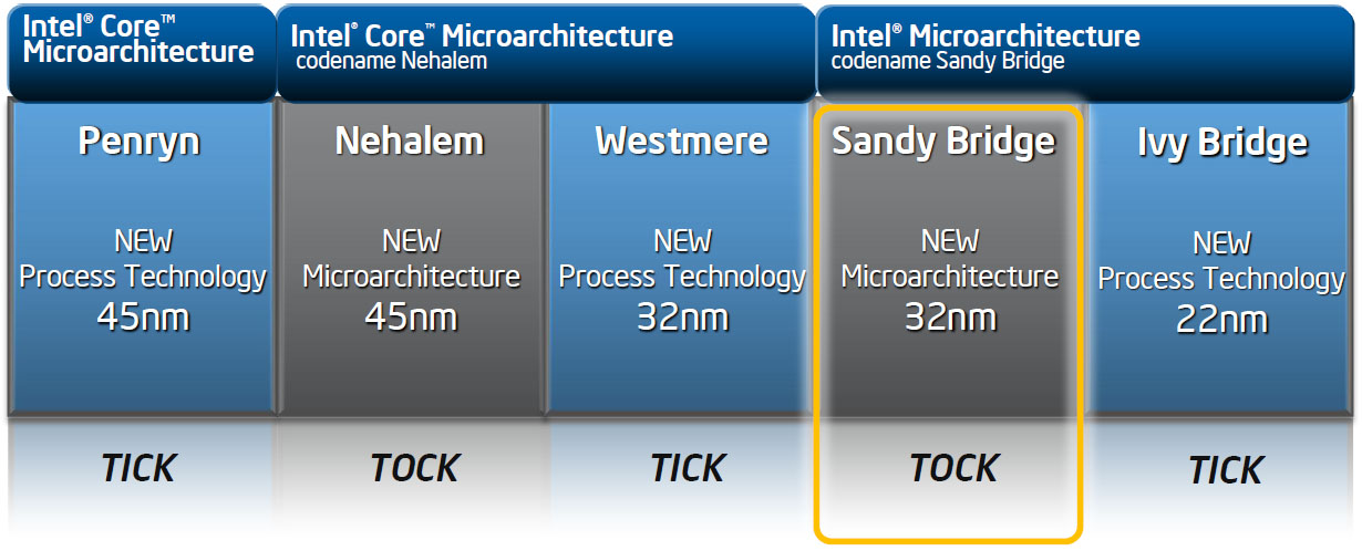
In comparison, the 45 nm Lynnfield design that served as the foundation for Intel’s Core i7-800- and Core i5-700-series chips measured a more portly 296 mm², despite the fact that it only consisted of 774 million transistors. Intel’s architects clearly owe much of what they were able to cram into Sandy Bridge to the engineers that brought the 32 nm node online for Westmere (tick), and then dialed in for today’s launch (tock).
The Cores
In its current state, Sandy Bridge-based processors are available with four cores (with and without Hyper-Threading) and two cores (dual-core models all have Hyper-Threading enabled). As you’ll see in the benchmarks, these cores are, clock-for-clock, more powerful than what we saw from Nehalem.
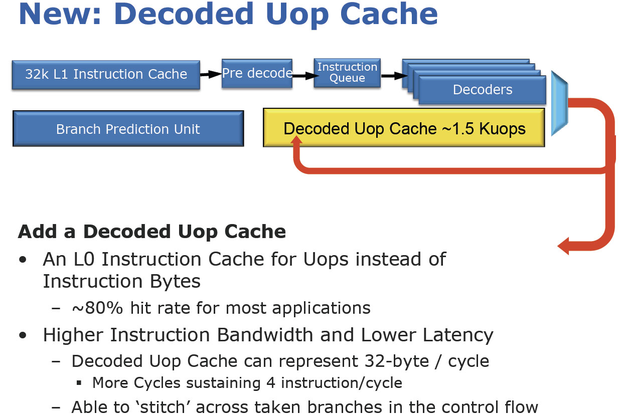
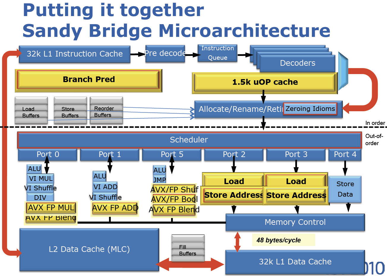
Still present are the 32 KB L1 instruction and data caches (along with 256 KB L2 cache per core), though Sandy Bridge now incorporates what Intel calls a L0 instruction cache that holds up to 1500 decoded micro-ops. This feature has the dual effect of saving power and improving instruction throughput. If the fetch hardware finds the instruction it needs in cache, it can shut down the decoders until they’re needed again. Intel also rebuilt Sandy Bridge’s branch prediction unit, improving its accuracy.
Get Tom's Hardware's best news and in-depth reviews, straight to your inbox.
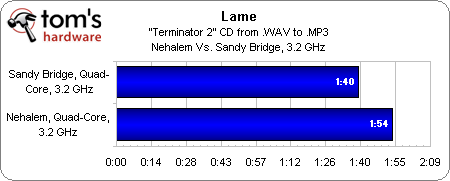
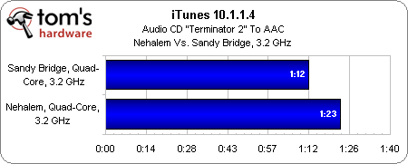
I ran these two single-threaded tests as a synthetic comparison of performance, clock for clock. Both quad-core chips are set to the same frequency with Turbo Boost and EIST disabled. As you can see, just the architectural shift makes a significant impact on Sandy Bridge's performance versus the Nehalem-based Lynnfield design.
Sandy Bridge-based processors are the first to support Advanced Vector Extensions (AVX), a 256-bit instruction set extension to SSE (AMD will also support AVX in its upcoming Bulldozer processor architecture). The impetus behind AVX comes from the high-performance computing world, where floating-point-intensive applications demand more horsepower than ever. To that end AVX’s impact on Sandy Bridge will very likely be limited. Intel does, however, expect that audio processing and video editing applications should eventually be optimized to take advantage of AVX (along with the financial services analysis and engineering/manufacturing software that AVX is really designed to target). Unfortunately, there aren't any real-world apps optimized for AVX that we can test as a gauge of the capability's potential.
Naturally, a lot of implementation work went into enabling AVX, including a transition from a retirement register file to a physical register. This allows operands to be stored in the register file, rather than traveling with micro-ops through the out-of-order engine. Intel used the power and die size savings enabled by the physical register to also significantly increase buffer sizes, more efficiently feeding its beefier floating-point engine.
The Cache
As a consequence of increased integration, Intel had to address the ways bits and pieces of its processor were accessing the last-level cache (in Sandy Bridge, it’s the L3).
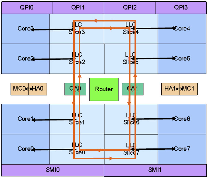
Back in the days of Bloomfield, Lynnfield, and Clarkdale, a four-core (and even six-core, in Westmere) ceiling meant that each physical core could have its own connection to that shared cache. The Xeon 7500-series processors were designed to be more scalable, though, and currently-shipping models feature as many as eight cores per CPU. Built the same way, that’d be an exorbitant number of traces between each core and the last-level cache. So, Intel adopted a ring bus that, in those enterprise environments, allows the company to keep scaling core count without the logistics getting out of control.
Earlier this year, I had the chance to talk to Sailesh Kottapalli, a senior principle engineer at Intel, who explained that he’d seen sustained bandwidth close to 300 GB/s from the Xeon 7500-series’ LLC, enabled by the ring bus. Additionally, Intel confirmed at IDF that every one of its products currently in development employs the ring bus. Think we’re going to see a continued emphasis on adding cores and other platform components directly to the CPU die? I’d say that’s a fair assumption.
Of course, Intel wasn’t worried about higher core count on the mainstream desktop version of Sandy Bridge. Rather, it was the on-die graphics engine that compelled a similar shift to the ring bus architecture, which now connects the graphics, up to four processing cores, and the system agent (formerly referred to as uncore) with a stop at each domain. Latency is variable, since each component takes the shortest path on the bus; overall, though it’s always going to be lower than a Westmere-based processor.
At the end of the day, the ring bus’ most significant contribution is going to be the performance it facilitates in graphics workloads.
Current page: Inside Of Sandy Bridge: Cores And Cache
Prev Page Core i7-2600K, Core i5-2500K, Core i5-2400, And Core i3-2100 Reviewed Next Page The System Agent And Turbo Boost 2.0-
cangelini MoneyFace pEditor, page 10 has mistakes. Its LGA1155, not LGA1555.Reply
Fixed, thanks Money! -
juncture "an unlocked Sandy Bridge chip for $11 extra is actually pretty damn sexy."Reply
i think the author's saying he's a sexually active cyberphile -
fakie Contest is limited to residents of the USA (excluding Rhode Island) 18 years of age and older.Reply
Everytime there's a new contest, I see this line. =( -
englandr753 Great article guys. Glad to see you got your hands on those beauties. I look forward to you doing the same type of review with bulldozer. =DReply -
joytech22 Wow Intel owns when it came to converting video, beating out much faster dedicated solutions, which was strange but still awesome.Reply
I don't know how AMD's going to fare but i hope their new architecture will at least compete with these CPU's, because for a few years now AMD has been at least a generation worth of speed behind Intel.
Also Intel's IGP's are finally gaining some ground in the games department. -
cangelini fakieContest is limited to residents of the USA (excluding Rhode Island) 18 years of age and older.Everytime there's a new contest, I see this line. =(Reply
I really wish this weren't the case fakie--and I'm very sorry it is. We're unfortunately subject to the will of the finance folks and the government, who make it hard to give things away without significant tax ramifications. I know that's of little consolation, but that's the reason :(
Best,
Chris -
LuckyDucky7 "It’s the value-oriented buyers with processor budgets between $100 and $150 (where AMD offers some of its best deals) who get screwed."Reply
I believe that says it all. Sorry, Intel, your new architecture may be excellent, but unless the i3-2100 series outperforms anything AMD can offer at the same price range WHILE OVERCLOCKED, you will see none of my desktop dollars.
That is all.
