AMD to broaden and specialize EPYC CPUs, already working on Zen 7 architecture — increased customization to better address evolving AI and cloud needs

EPYC Turin
AMD hints at broader Zen 6, Zen 7 server CPU lineup optimized for a broad range of AI and hyperscale workloads. (Image credit: AMD)

Modern data center workloads are very diverse, and so are the requirements of data center operators for their hardware, which is why virtually all hyperscale cloud service providers nowadays have their own custom silicon programs. In a bid to stay competitive in the coming years, AMD plans to expand its portfolio of CPUs for data centers that will be targeted at different workloads.

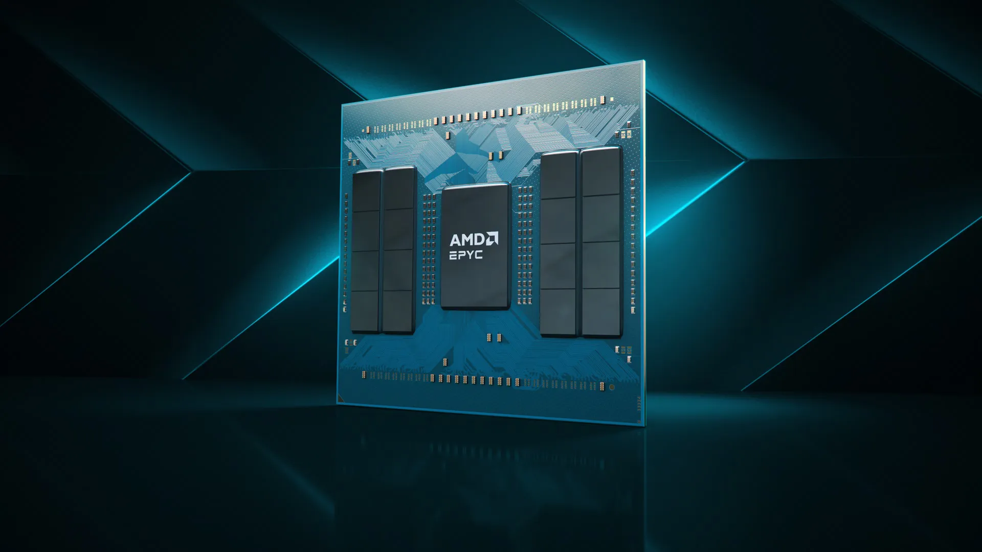
With the Zen 4-based 4th Generation EPYC family, AMD offers a variety of processors SKUs aimed at AI, cloud, enterprise, network/edge, and small business/hosted service providers. But with Zen 5, the family is somewhat narrower. AMD's messaging today suggests that the company is moving toward more segmented EPYC products, including workload-specific SKUs, potentially different core/cache/interconnect configurations, and CPUs tailored for inference clusters, orchestration, low-latency AI tasks, and GPU-heavy deployments. Specifically, Su also hinted that this expansion is going beyond Venice, which includes Zen 7 and probably Zen 8 microarchitectures.

"We are working with customers right now on beyond Venice and what we are doing in those architectures," Su said.

Latest Videos From

 "[The industry] is going to need a broad portfolio of CPUs, not all CPUs are the same," said Lisa Su, chief executive and chairman of AMD, during the company's earnings call with financial analysts and investors. "Frankly, you are going to need different CPUs for whether you are talking about general purpose operations or you are talking about head nodes or you are talking about agentic AI tasks."

During the Q&A, Su repeatedly emphasized that AMD no longer sees server CPUs as a single homogeneous category. Instead, the company now views the market as split into multiple workload-specific segments, including general-purpose compute, CPU head nodes for accelerators, and CPUs optimized for agentic AI workloads. However, AMD plans to offer differentiation even within these categories to address the particular needs of its customers more precisely.

"What we have been focused on is building, not just one type, but […] throughput optimized, power optimized, cost optimized, and AI infrastructure optimized [models] as we have done in the Venice family," Su said.

Indeed, when it comes to AMD's 6th Generation EPYC processors based on the Zen 6 microarchitecture, the company plans to offer its codenamed Venice CPU with up to 256 cores for general-purpose servers as well as codenamed Verona processors for AI infrastructure (previously, AMD only introduced Verano CPUs as the processor that will power its next-generation rack-scale AI solutions). We yet have to learn whether CPUs aimed at agentic AI workloads will use separate silicon configurations or will re-use what was originally intended for general-purpose servers, but with different clocks or cache configurations.

" The Venice family spans a broad set of CPUs optimized for throughput, performance per watt, and performance per dollar, including Verona, our first EPYC CPU purpose-built for AI infrastructure," Su said.

Considering the fact that AMD now expects the server CPU total available market to grow at a 35% compound annual growth rate and reach $120 billion by 2030, development of specialized models may be well justified even though CPU development in general and CPU implementation on leading-edge nodes in particular has become especially expensive in recent years.

So, while AMD did not formally announce any new CPU categories, its chief executive clearly signaled an ongoing expansion and specialization of EPYC offerings around AI infrastructure and other segments of the market.

Google Preferred Source

Follow Tom's Hardware on Google News, or add us as a preferred source, to get our latest news, analysis, & reviews in your feeds.

TOPICS
Anton Shilov
Contributing Writer

Anton Shilov is a contributing writer at Tom’s Hardware. Over the past couple of decades, he has covered everything from CPUs and GPUs to supercomputers and from modern process technologies and latest fab tools to high-tech industry trends.

  • GenericUser2001
    From the consumer side of things hopefully some of the specialization for different server workloads has a fair bit of crossover for everyday tasks. For example, the 3d cache on the x3d chips was originally intended for certain server workloads, but turned out to be really good for gaming too.
    Reply
  • DS426
    GenericUser2001 said:
    From the consumer side of things hopefully some of the specialization for different server workloads has a fair bit of crossover for everyday tasks. For example, the 3d cache on the x3d chips was originally intended for certain server workloads, but turned out to be really good for gaming too.
    Not disagreeing, but the GPU is the bottleneck in gaming, not the CPU. To your point, 3D cache put AMD's CPU's on top in gaming, and now they just need that 3D cache moment with GPU's. They don't even have to beat nVidia at the very top end, but a strong high-end performer for hundreds less is what many are craving.
    Reply
  • usertests
    There are tons of options on the table with multiple types of chiplets available. They are apparently going to use multiple I/O chiplets to control how many channels/lanes can be offered. There's supposed to be a 36-core Zen 7 chiplet with L3 cache disaggregated from it (related to but distinct from X3D). Maybe they can mix 8-core, 16-core, and 36-cores at will. Possibly add a graphics chiplet like the MI300A. It could get dizzying.

    If they don't want to offer dozens upon dozens of SKUs, they could allow the big hyperscaler/AI customers to customize their Epyc to the extent possible.
    Reply
  • bit_user
    DS426 said:
    Not disagreeing, but the GPU is the bottleneck in gaming, not the CPU.
    To the extent that the CPU is still a bottleneck in gaming, Chips & Cheese found that Zen 5 is predominantly front-end bound on the 3 games they analyzed. If Zen 6 improves front-end throughput (which I think is consistent with the rumors?), then it could actually make a pretty big dent in what CPU bottlenecks remain.
    Source: https://chipsandcheese.com/p/running-gaming-workloads-through
    DS426 said:
    To your point, 3D cache put AMD's CPU's on top in gaming, and now they just need that 3D cache moment with GPU's.
    The first big step towards that was RDNA 2's Infinity Cache. RDNA 3 was rumored to have bumps for stacking a cache die atop the MCDs, but it never happened for either market or technical reasons.

    RDNA 4 had a canceled flagship that was rumored to make even more aggressive use of die stacking. I think we might yet see them implement that vision, but no guesses as to whether it'll happen in RDNA 5.
    Reply
  • usertests
    bit_user said:
    RDNA 4 had a canceled flagship that was rumored to make even more aggressive use of die stacking. I think we might yet see them implement that vision, but no guesses as to whether it'll happen in RDNA 5.
    Based on MLID leaks, they could be ditching Infinity Cache (L3) entirely in favor of embiggened L2 cache, closer to what Nvidia uses. And no die stacking detected, but GPU chiplets that can be shared between mobile APUs, gaming dGPUs, the Xbox Helix, and workstation/accelerators.

    AT4 = 24 CUs, 10 MiB L2 cache (128-bit Medusa Halo Mini)
    AT2/AT3? = 44-64 CUs, 16-24 MiB L2 cache (256/384-bit Medusa Halo with 48 CUs, 20 MiB L2)
    AT0 = 138-184 CUs, 40-64 MiB L2 cache

    I'm using these two leaks. There are some discrepancies (more than I remembered!) which I attempted to resolve above.

    uLsykckkoZU:860View: https://youtu.be/uLsykckkoZU?t=860 (July 2025)

    https://www.reddit.com/r/pcmasterrace/comments/1mydfvj/leaks_of_rdna5_new_gpus_coming_in_2027_possible/
    K0B08iCFgkk:1183View: https://youtu.be/K0B08iCFgkk?t=1183 (August 2025)

    https://www.notebookcheck.net/Next-gen-AMD-RDNA-5-desktop-GPUs-leak-Mid-range-AT3-GPU-features-48-CUs-and-massive-384-bit-bus.1093904.0.html

    It remains to be seen how discrete desktop GPUs would handle these changes, but they should be great for Medusa Halo Mini, which is presumed to be the Strix Point successor. Strix Point has only 2 MiB L2 cache for graphics, while Panther Lake has a gigantic 16 MiB.

    AT4 was estimated as having RTX 3060-4060 raster performance, while using at least 12 GB of cheap LPDDR5X. It could be made into a good dGPU for the low-end.

    AT0 could allow an effective RTX 6090 competitor. But don't hold your breath.
    Reply
  • CPUvsGPU
    It remains to be seen how discrete desktop GPUs would handle these changes, but they should be great for Medusa Halo Mini, which is presumed to be the Strix Point successor. Strix Point has only 2 MiB L2 cache for graphics, while Panther Lake has a gigantic 16 MiB.
    For 8K resolution need frame bufer of size 7,680*4,320 *3 (colours, each 8 bit) = 99,532,800 bytes or about 99.5 Mbytes. To take inforamtion so fast from frame bufer and to output it to monitor need very fast VRAM with latencies about 99,532,800/3 (if 24 bits outputed at a time) = 33,177,600. If monitor output rate is 60 Hz, then 1/(33,177,600 * 60) = 5.02347 *10^(-10). It is 0.5 nanosecond. This equal to VRAM "latency frequency" 1/(5.02347 *10^(-10)) = 1,990,656,000 Hz or 1.99 GHz, almost 2 GHz. Thus looks like VRAM don't have issues with latency. Because noramal RAM latency (like DDR4), like CAS latency is about 13 ns or about 70-100 MHz. Or GPU's VRAM must have about 100 MB cache for 8K frame bufer, if no compresion of frames. For good frames quality compresion can't be more than 4-5 times like it is on .PNG image files. Even .jpg files compress .bmp image only 15-20 times, which is not acceptable and can be computationaly too expensive. Thus at least 5 MB of SRAM VRAM needed for jpg quality 8K gaming without upscaling, because shown frames of say desktop and windowses can be a bit blured.
    EDIT: To get RAM "latency frequency" need to divide RAM frequency by CAS latency. For example DDR5-6200 CL30 have frequency 3100 MHz. Then RAM "latency frequency" is 3100/30 = 103.33 MHz. And then DDR5-6200 latency is 1/(103,333,333) = 9.6774 * 10^(-9) (s) or about 9.7 ns. The bigger CAS (Column Address Strobe) latency in cycles, the more cycles CPU have to wait for RAM to respond for sending or retrieving data to/from RAM.
    Reply
  • bit_user
    CPUvsGPU said:
    To take inforamtion so fast from frame bufer and to output it to monitor need very fast VRAM with latencies about ...
    No, it's not a latency thing. The display controller can queue up DMA transfers to fetch blocks of framebuffer data, in advance. So, you only need to worry about bandwidth. That shouldn't be a problem, since 8k @ 60 Hz is only 5.97 GB/s (at 24-bit without DSC).

    CPUvsGPU said:
    For good frames quality compresion can't be more than 4-5 times like it is on .PNG image files.
    Well, typical compression ratios for DSC are only in the realm of 3:1, according to wikipedia:
    https://en.wikipedia.org/wiki/Display_Stream_Compression
    Reply
  • CPUvsGPU
    No, it's not a latency thing. The display controller can queue up DMA transfers to fetch blocks of framebuffer data, in advance. So, you only need to worry about bandwidth.
    Yes, that should do with 16 blocks of 24 bits each. 16*24 = 384 bits. And 16 *80 MHz (latency) = 1280 MHz, but maybe VRAM latency smaller that 13 ns. And RAM burst lenght can play vital role. Like it was 8 for older VRAM and 16 or 32 for newer VRAM.
    Burst lenght means, it fetching information from RAM cells, from 8 RAM addresses at once with burst lenght 8. Like from addresses from 3001 to 3008 in single RAM address access, in next RAM address access, bits fetched from RAM addresses 3009 to 3016. This is possible, beacause single RAM address is treated like 8 RAM addresses, where is special engine (inside RAM chips) which fetching from 8 RAM addresses data and fast transmits data to GPU or CPU by normal peaces defined by RAM data bus (like 128 bits or 64 bits). In over words speaking internal data bus wide is 8 times bigger with burst lenght 8 than with burst lenght of 1 (1024 bit instead of 128 bit). Too bad there is not much hystorical information about burst lenght incorporation into RAM for diferent timelines. Like what was burst lenght for DDR, what was for DDR2, for DDR3? Or SDR?
    Reply
  • bit_user
    CPUvsGPU said:
    And RAM burst lenght can play vital role. Like it was 8 for older VRAM and 16 or 32 for newer VRAM.
    Yeah, regular DDR5 supports two burst lengths: 16 x 32-bits and 8 x 32-bits. So, that works out to 64 bytes (standard cacheline size) or 32 bytes. The short bursts are called "chop" bursts, I guess because the burst is chopped off early.
    https://www.rambus.com/blogs/get-ready-for-ddr5-dimm-chipsets/
    I don't know about LPDDR5 or MRDDR5. I had the impression that the burst lengths would double, in MR-DIMMs, but I'm not totally sure about that.

    CPUvsGPU said:
    Too bad there is not much hystorical information about burst lenght incorporation into RAM for diferent timelines. Like what was burst lenght for DDR, what was for DDR2, for DDR3? Or SDR?
    I didn't look for anything older, but the above link compares DDR4 vs DDR5.
    Reply