Overview
The VT82C580VP Apollo-VP-1 is a high performance, cost-effective and energy efficient chip set for the implementation of PCI/ISA desktop and notebook personal computer systems based on the 64 bit Pentium/AMD5K 86/Cyrix8X 86 super-scalar processors.
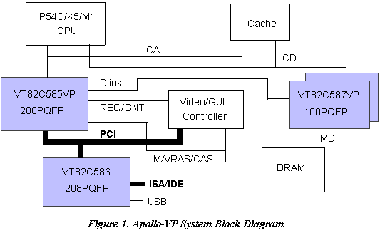
The VT82C580VP chip set consists of the VT82C585VP system controller, the VT82C586 PCI to ISA bridge, and two instances of the VT82C587VP data buffers. The secondary (L2) cache is based on burst synchronous (pipelined or non-pipelined) SRAM, asynchronous SRAM or cache module from 256 kB to 2 MB. For burst synchronous SRAMs, 3-1-1-1-1-1-1-1 timing can be achieved for both read and write transactions at 66/75 MHz. Four cache lines (16 quadwords) of CPU/cache to DRAM write buffers with concurrent write-back capability are included in the VT82C587VP data buffer chips to speed up the cache read and write miss cycles. These buffers also minimizes DRAM utilization and allows minimum performance degradation due to unified memory architecture with the video/GUI controller.
The VT82C580VP supports six banks of DRAMs up to 512 kB. The DRAM controller supports Standard Page Mode DRAM, EDO-DRAM, Burst EDO-DRAM and Synchronous DRAM in a flexible mixed/match manner. The Burst-EDO and Synchronous DRAM allows zero wait state bursting between the DRAM and the VT82C587VP data buffers at 66 MHz. The six banks of DRAM can be composed of arbitrary mixture of 1M/2M/4M/8M/16MxN DRAMs. Each bank may be populated with either 32bit or 64bit data width.
The VT82C580VP supports 3.3/5v 32 bit PCI bus with 64 bit to 32 bit data conversion. Five levels (doublewords) of post write buffers are included to allow for concurrent CPU and PCI operation. Consecutive CPU addresses are converted into burst PCI cycles with Byte merging capability for optimal CPU to PCI throughput. For PCI master operation, Sixty-four levels (doublewords) of post write buffers and thirty two levels (doublewords) of prefetch buffers are included for concurrent PCI bus and DRAM/cache accesses. The chipset also supports enhanced PCI bus commands such as Memory-Read-Line, Memory-Read-Multiple and Memory-Write-Invalid commands to minimize snoop overhead. In addition, the chipset supports advanced features such as snoop ahead, snoop filtering, L1 write-back forward to PCI master and L1 write-back merged with PCI post write buffers to minimize PCI master read latency and DRAM utilization. The VT82C586 PCI to ISA bridge supports four levels (doublewords) of line buffers, type F DMA transfers and delay transaction to allow efficient PCI bus utilization and (PCI-2.1 compliant). The VT82C586 also includes integrated keyboard controller with PS2 mouse support, integrated DS12885 style real time clock with extended 128 Byte CMOS RAM, integrated master mode enhanced IDE controller with full scatter and gather capability and extension to 33 MB/sec ATA-33 transfer rate, integrated USB interface with root hub and two function ports with built-in physical layer transceiver, and OnNow/ACPI compliant advanced configuration and power management interface. A complete main board can be implemented with only six TTLs. ]
The VT82C580VP is ideal for high performance, high quality, high energy efficient and high integration desktop and notebook PCI/ISA computer systems.