Features

- PCI/ISA Green PC Ready
- High Integration
- VT82C595 system controllerVT82C586 PCI to ISA bridgeSix TTLs for a complete main board implementation
- Flexible CPU Interface
- 64 bit P54CTM, K5TM and M1TM CPU interfaceCPU external bus speed up to 75 MHz (internal 200 MHz and above)Supports CPU internal write-back cacheConcurrent CPU/cache and PCI/DRAM operationSystem management interrupt, memory remap and STPCLK mechanismCyrix M1 linear burst supportCPU NA#/Address pipeline capability
- Advanced Cache Controller
- Direct map write back or write through secondary cacheBurst Synchronous Cache SRAM supportFlexible cache size: 0K/256K/512K/1M/2 MB32 Byte line size to match the primary cacheIntegrated 10 bit tag comparator3-1-1-1 read/write timing for Burst Synchronous SRAM access at 66 MHz3-1-1-1-1-1-1-1 back to back read timing for Burst Synchronous SRAM access at 66 MHzSustained 3 cycle write access for Burst Synchronous SRAM access or CPU to DRAM and PCI bus post write buffers at 66 MHzData streaming for simultaneous primary and secondary cache line fillSystem and video BIOS cacheable and write-protectProgrammable cacheable region and cache timingOptional combined tag and alter bit SRAM for write-back scheme
- Fast DRAM Controller
- * Fast Page Mode/EDO/Burst EDO/Synchronous-DRAM support in a mixed combinationMixed 256K/512K/1M/2M/4M/8M/16MxN DRAMs6 banks up to 512 MB DRAMs (maximum four banks of Synchronous DRAM)Flexible row and column addresses64 bit or 32 bit data width in arbitrary mixed combination3.3v and 5v DRAM without external transceiversOptional Parity and ECC (one bit error correction and multi-bit error detection) for DRAM integrityFour Cache lines (16 quadwords) of CPU/cache to DRAM write buffersConcurrent DRAM writebackSpeculative DRAM accessRead around Write capability for non-stalled CPU readBurst read and write operation4-2-2-2 on page, 7-2-2-2 start page and 9-2-2-2 off page timing for EDO DRAMs at 50/60 MHz5-2-2-2 on page, 8-2-2-2 start page and 11-2-2-2 off page timing for EDO DRAMs at 66 MHz5-1-1-1 on page, 8-1-1-1 start page and 10-1-1-1 off page timing for Burst EDO DRAMs at 66 MHz5-2-2-2-3-1-2-2 back-to-back access for EDO DRAM at 66 MHz5-1-1-1-3-1-1-1 back-to-back access for BEDO DRAM at 66 MHzBIOS shadow at 16 kB incrementSystem management memory remappingDecoupled and burst DRAM refresh with staggered RAS timingProgrammable refresh rate, CAS-before-RAS refresh and refresh on populated banks only
- Unified Memory Architecture
- Supports VESA UMA handshake protocolCompatible with major video/GUI productsDirect video frame buffer accessSatisfies maximum latency requirement from REQ# to GNT# and from GNT# to REQ#
- Intelligent PCI Bus Controller
- 32 bit PCI interfaceSupports 66 MHz and 3.3v/5v PCI busPCI master snoop ahead and snoop filteringPCI master Peer ConcurrencySynchronous Bus to CPU clock with divide-by-two from the CPU clockAutomatic detection of data streaming burst cycles from CPU to the PCI busFive levels (double-words) of CPU to PCI posted write buffersByte merging in the write buffers to reduce the number of PCI cycles and to create further PCI bursting possibilitiesZero wait state PCI master and slave burst transfer ratePCI to system memory data streaming up to 132 MByte/secSixty-four levels (double-words) of post write buffers from PCI masters to DRAMThirty-two levels (double-words) of prefetch buffers from DRAM for access by PCI mastersEnhanced PCI command optimization (MRL, MRM, MWI, etc)Complete steerable PCI interruptsSupports L1 write-back forward to PCI master read to minimize PCI read latencySupports L1 write-back merged with PCI master post-write to minimize DRAM utilizationProvides transaction timer to fairly arbitrate between PCI mastersPCI-2.1 compliant
- Enhanced Master Mode PCI IDE Controller
- Dual channel master mode PCI supporting four Enhanced IDE devicesTransfer rate up to 22 MB/sec to cover PIO mode 4 and Multiword DMA mode 2 drivers and beyondSixteen levels (doublewords) of prefetch and write buffersInterlaced commands between two channelsBus master programming interface for ATA controllers SFF-8038 rev.1.0 compliantFull scatter and gather capabilitySupport ATAPI compliant devicesSupport PCI native and ATA compatibility modesComplete software driver support
- Universal Serial Bus Controller
- USB v1.0 and Intel Universal HCI v1.1 compatibleEighteen levels(doublwords) of data FIFOsRoot hub and two function parts with built-in physical layer transceiversLegacy keyboard and PS/2 mouse support
- Plug and Play Controller
- Dual interrupt and DMA signal steering with plug and play controlMicrosoft Windows 95TM and plug and play BIOS compliant
- Sophisticated Power Management Unit
- Normal, doze, sleep, suspend and conserve modesSystem event monitoring with two event classesOne idle timer, one peripheral timer and one general purpose timerMore than ten general purpose Input/Output portsSix external event input ports with programmable SMI conditionComplete leakage control when external component is in power off statePrimary and secondary interrupt differentiation for individual channelsClock stretching, clock throttling and clock stop controlMultiple internal and external SMI sources for flexible power management modelsTwo programmable output portsAPM 1.2 compliant
- PCI to ISA Bridge
- Integrated 82C206 peripheral controllerIntegrated keyboard controller with PS2 mouse supportsIntegrated DS12885 style real time clock with extended 128 Byte CMOS RAMIntegrated USB (universal serial bus) controller with hub and two function portsIntegrated master mode enhanced IDE controller with enhanced PCI bus commandsPCI-2.1 compliant with delay transactionFour double-word line buffer between PCI and ISA busSupports type F DMA transfersFast reset and Gate A20 operationEdge trigger or level sensitive interruptFlash EPROM and combined BIOS support
- Built-in nand-tree pin scan test capability
- 0.6um mixed voltage, high speed and low power CMOS process
- 328 pin BGA Package for VT82C595
- 208 pin PQFP for VT82C586
Overview
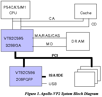
The VT82C590 Apollo-VP2 is a high performance, cost-effective and energy efficient chip set for the implementation of PCI/ISA desktop and notebook personal computer systems based on the 64 bit P54C/Pentium/K5/M1 super-scalar processors. CPU and cache interface is supported up to 75 MHz CPU external bus speed (with CPU internal speed up to 200 MHz and above). The Apollo-VP2 chip set consists of the VT82C595 system controller (328 pin BGA) and the VT82C586 PCI to ISA bridge (208 pin PQFP) The VT82C595 system controller provides superior performance between the CPU, optional synchronous cache, DRAM and the PCI bus with pipelined, burst and concurrent operation. The VT82C586 PCI to ISA bridge includes integrated 206-style IPC (DMA, interrupt controller and timer), integrated keyboard controller with PS2 mouse support, integrated DS12885 style real time clock with extended 128 Byte CMOS RAM, integrated master mode enhanced IDE controller with full scatter and gather capability, and integrated USB (universal serial bus) interface with root hub and two function ports with built-in physical layer transceiver. A complete main board can be implemented with only six TTLs. Please refer to Figure 1 for the system block diagram.
The secondary (L2) cache is based on Burst Synchronous (Pipelined or non-pipelined) SRAM from 256 kB to 2 MB. The VT82C590 supports CPU address pipelining to achieve back to back 3-1-1-1-1-1-1, and sustained three cycle single write timing at 66 MHz. Four cache lines (16 quadwords) of CPU/cache to DRAM post write buffers are included in the VT82C595 system controller to allow sustained 3-1-1-1 cache miss write and bursting into the DRAM for optimal system performance.
The VT82C590 supports six banks of DRAMs up to 512 kB. The DRAM controller supports Standard Page Mode DRAM, EDO-DRAM, Burst EDO-DRAM and Synchronous DRAM in a flexible mixed/match manner. The Burst-EDO and Synchronous DRAM allows zero wait state bursting between the DRAM and the integrated data buffers at 66 MHz. The six banks of DRAM can be populated with an arbitrary mixture of 256K/512K/1M/2M/4M/8M/16MxN DRAMs with flexible combination of 32bit or 64bit data width.
The VT82C590 supports 3.3/5v 32 bit PCI bus with 64 bit to 32 bit data conversion. Five levels (doublewords) of post write buffers are included to allow for concurrent CPU and PCI operation. Consecutive CPU addresses are converted into burst PCI cycles with Byte merging capability for optimal CPU to PCI throughput. Sixty-four levels (doublewords) of post write buffers and thirty two levels (doublewords) of prefetch buffers are included for concurrent PCI bus and DRAM/cache accesses. The chipset also supports enhanced PCI bus commands such as Memory-Read-Line, Memory-Read-Multiple and Memory-Write-Invalid commands to minimize snoop overhead. In addition, the chipset supports advanced features such as snoop ahead, snoop filtering, L1 write-back forward to PCI master and L1 write-back merged with PCI post write buffers to minimize PCI master read latency and DRAM utilization. The VT82C586 PCI to ISA bridge supports four levels (doublewords) of line buffers, type F DMA transfers and delay transaction to allow efficient PCI bus utilization and (PCI-2.1 compliant).
The integrated master mode IDE controller supports a dual channel/four device enhanced IDE bus with sixteen levels of double-word prefetch and write buffers. The data bus, control signals, write buffers and prefetch buffers are separated from those of the PCI bus so that performance and electrical loading are optimized. The command and recovery time of each IDE device can be individually programmed in units of PCI bus clock to achieve optimal speed of the device up to >22 MB/s. Other features of the IDE controller include interlaced dual channel commands, full scatter and gather capability, bus master programming interface for ATA controllers SFF-8038 compliant (Windows 95 built-in driver compliant) and complete software driver support.
The VT82C590 integrates the USB (universal serial bus) host controller with root hub and two function ports with integrated physical layer transceiver. The host interface is register compatible with the Intel Universal HCI specification 1.1 to allow seamless integration with the Microsoft Windows 95 (and NT) operating system. Eighteen levels of data FIFOs with scatter and gather capabilities are included to further enhance the overall system performance.
The integrated power management unit offers the following modes: normal, doze, sleep, suspend and conserve. To determine the power management mode, the power management unit monitors IO events, interrupt, DMA and PCI master request signals to detect the status of system activity. Each event can be turned off or assigned to one of two event classes tracked by an idle timers, a peripheral timer and a general purpose timer. The system management interrupt (SMI) may be triggered by multiple sources including time-out of individual timers, occurrence of system activities, external input and software programming for flexible applications. Clock throttling, IO and power control are functions performed by the SMI routine. The power management unit is APM 1.2 compliant.
The VT82C590 is ideal for high performance, high quality, high energy efficient and high integration desktop and notebook PCI/ISA computer systems.