SandForce Demos 24-nm MLC NAND from Toshiba
SandForce is currently demoing its latest SF-2000 series controller with Toshiba's new 24-nm MLC Toggle NAND Flash memory at the Flash Memory Summit in California.
SandForce said on Tuesday that it's currently demonstrating the use of its latest SF-2000 series SSD controller with Toshiba’s new 24-nm MLC Toggle Flash memory in a 2.5-inch SSD form factor. The union is producing balanced read and write speeds up to 500 MB/s and up to 60,000 IOPS with Toshiba's memory operating at 166 MT/s.
So what does this mean for consumers? The combination enables "SandForce Driven" SSD manufacturers to produce more affordable SSD products which will further accelerate adoption in the enterprise, client, and industrial computing markets that demand optimized reliability, performance, and power efficiency.
"Our award winning DuraClass technology includes a number of features enabling the industry’s highest level of reliability, endurance, performance, and power efficiency in a single SSD Processor solution," said Thad Omura, vice president of marketing at SandForce. "We worked closely with Toshiba to expand DuraClass with additional advanced read recovery techniques vital to the successful operation of SSDs that use more aggressive NAND Flash process nodes."
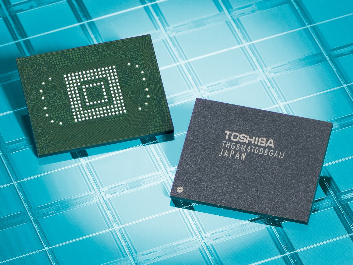
Article continues belowToshiba America Electronic Components, Inc. (TAEC) originally introduced the 24-nm toggle-mode double data rate (DDR) NAND flash memory modules just weeks ago, ranging from 2 GB (Q1 2012) to 128 GB (Q4 2011). According to the company, these modules feature the world's smallest geometry e-MMC, one of the highest capacities achieved in the industry, and offer full compliance with the JEDEC e-MMC Version 4.41 standard.
"Toshiba was the first company to succeed in combining 16 pieces of 64 Gbit die in e-MMC to achieve 128 GB of memory by applying advanced chip thinning and layering technologies to realize individual chips that are only 30 micrometers thick," the company said. "Full compliance with the JEDEC e-MMC Version 4.41 (V4.41) standard for embedded MultiMediaCards supports standard interfacing and simplifies product design-in, reducing development burdens on product manufacturers."
For those who want to see the SandForce controller and Toshiba’s new NAND in action together, the demo will be shown during the Flash Memory Summit exhibition hours at booth #407-409 located in the Santa Clara Convention Center. The convention is currently underway and will conclude on Thursday, August 11.
Get Tom's Hardware's best news and in-depth reviews, straight to your inbox.

Kevin Parrish has over a decade of experience as a writer, editor, and product tester. His work focused on computer hardware, networking equipment, smartphones, tablets, gaming consoles, and other internet-connected devices. His work has appeared in Tom's Hardware, Tom's Guide, Maximum PC, Digital Trends, Android Authority, How-To Geek, Lifewire, and others.
-
warmon6 ReplyToshiba America Electronic Components, Inc. (TAEC) originally introduced the 24-nm toggle-mode double data rate (DDR) NAND flash memory modules just weeks ago, ranging from 2 GB (Q1 2012) to 128 GB (Q4 2011).
could be just me but is there something wrong with the bold section. i think the quarter/year need to be switched around. -
burnley14 Isn't the current generation 28nm? So this is a relatively minor die shrink, correct?Reply -
agnickolov burnley14Isn't the current generation 28nm? So this is a relatively minor die shrink, correct?No, it's 25nm. The advance is even more minuscule than you think.Reply -
rantoc agnickolovNo, it's 25nm. The advance is even more minuscule than you think.Reply
I doubt they want to push the shrinking to much and to fast with Nand, the numbers of erase cycles lowers with each round of shrinking and needs to be resolved. SSD have started to set sails for real but reliability is a major concern and shrinking it to much to quickly will lead to justifying those concerns when SSD's start to fail on larger scales. -
mikem_90 burnley14Isn't the current generation 28nm? So this is a relatively minor die shrink, correct?Reply
Pretty much. We're already operating under the resolution of the wavelength of light, though I hope better lithography techniques would be more center to upcoming advances. Like the 3D gates and fins used in the upcoming Intel chips.
I doubt we'll see too much focus on lithography shrinkage over time. Maybe if IBM ever got their x-ray lithography technology off the ground, but you kind of have to use a mask the size of the item you want to make, focusing X-rays is not trivial. -
ProDigit10 We're getting slowly into the territory, where we should start worrying about the SSD's lifetime!Reply
24nm is very small, and perhaps, if you're lucky they will last a good 20 years, but there's no guarantee that it will!
The smaller the transistors, the easier it is to break them with power spikes, magnetic fluxes, and perhaps even mechanical shocks... -
dalauder ProDigit10We're getting slowly into the territory, where we should start worrying about the SSD's lifetime!Aren't tons of people already worried about SSD lifetimes? That's why people talk about over-provisioning. Most HDDs don't last 12 years, so I'm not too worried about 20 year lifetimes. I'm more worried about the apparent low reliability of SSDs compared to HDDs.Reply
