Ivy Bridge CPU Torndown, Photographed, Tri-Gates Revealed
Media and Consulting firm UBM TechInsights says it was able to obtain a sample of Intel's 22 nm Ivy Bridge processor ahead of the CPU's official launch.
The company deconstructed the chip and performed a structural analysis that is planned to be released in two parts on May 4 and May 18. Some images have been released by EETimes, which is also part of UBM.
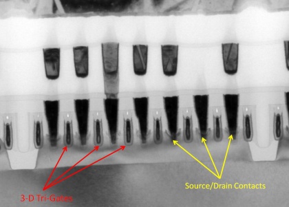
According to TechInsights, the 3.3 GHz Core i5-3550 was packaged in Malaysia and has a die size of 170 mm2, which is down from 208 mm2 for a comparable Sandy Bridge processor. The company analyzed the processor using electron microscopy as well as "x-ray techniques" and spreading resistance profiling and said it discovered 90 nm gate pitches in the embedded SRAM, but also 22 nm gate lengths in the logic areas.
A published picture confirms Intel's 22 nm tri-gate 3D transistors.
Article continues belowGet Tom's Hardware's best news and in-depth reviews, straight to your inbox.

Douglas Perry was a freelance writer for Tom's Hardware covering semiconductors, storage technology, quantum computing, and processor power delivery. He has authored several books and is currently an editor for The Oregonian/OregonLive.
-
atikkur alxianthelastCan't wait to run crysis 3 on this.Reply
will be the same, crysis is already cheap n light. -
josejones I'd like to find out if the TDP specs have changed in the new Ivy Bridge CPU going from 77 watts up to 95 watts or not?Reply
Intel’s Ivy Bridge Core i7 3770K Retail Box Leaked – TDP Raised to 95W?
If so, will it only be an issue with the k overclock versions or will it be an issue with all Ivy Bridge CPU's across the board i.e. k, s, t, and the regular 3770 and 3570's?
-
DavidC1 nforce4maxInteresting mix of process tech. 90nm and 22nm tri gate.Reply
Just like your size can not be determined by height alone(height, width, thickness), the same is with transistors.
22nm is size of the gate, 90nm refers to the distance between transistors. Way different. -
Kryan frozoniccheap n light..... nice, this proves we have advanced a lot! 4 years ago that game was unplayable even with Quad sli @ 1080p with maximun detailsReply
This has nothing to do with...anything here really. Crysis 2 was dumbed down to keep it even with consoles, as well as featuring better optimization than the original Crysis (which was a beast, but by NO means needed quad SLI to be played at max graphics, unless you were using cards that were 1-2 years old at that stage).
Related to the article: I want me an electron microscope! :D -
apache_lives josejonesI'd like to find out if the TDP specs have changed in the new Ivy Bridge CPU going from 77 watts up to 95 watts or not? Intel’s Ivy Bridge Core i7 3770K Retail Box Leaked – TDP Raised to 95W?If so, will it only be an issue with the k overclock versions or will it be an issue with all Ivy Bridge CPU's across the board i.e. k, s, t, and the regular 3770 and 3570's?Reply
K series are always higher -- normal. Standard cpus should be less ~65-80w

