Fujitsu flaunts massive 144-core Monaka Arm chip — 2nm and 5nm chiplets, 3D-stacked CPU cores over memory
Fujitsu shows off a mechanical sample of Monaka.

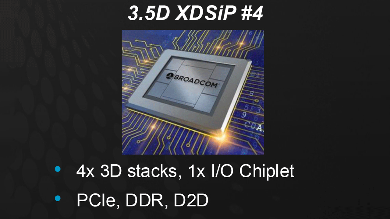
Fujitsu has demonstrated a mechanical sample of its Armv9-based 144-core Monaka processor for data centers, revealing some details. Less than a week ago, it disclosed that it is being developed with Broadcom and relies on its 3.5D eXtreme Dimension System in Package platform. Satoshi Matsuoka, director of the RIKEN Center for Computational Science (R-CCS) and a professor at Tokyo Tech, published the image.
Fujitsu's Monaka is a huge CoWoS system-in-package (SiP) that has four 36-core compute chiplets made on TSMC's N2 process technology housing 144 Armv9-based cores with enhancements that are stacked on top of SRAM tiles in a face-to-face (F2F) manner using hybrid copper bonding (HCB). The SRAM tiles (essentially huge caches) are produced on TSMC's N5 process technology. The compute and cache stacks are accompanied by a relatively colossal I/O die that integrates a memory controller, PCIe 6.0 lanes with CXL 3.0 on top to connect accelerators and extenders, and other interfaces that one comes to expect from a datacenter-grade CPU.
Just as expected, being aimed at a broad range of data center workloads, Monaka does not rely on high bandwidth memory but will use mainstream DDR5 DRAM, possibly in its MR-DIMM and MCR-DIMM implementations, to provide enough capacity and achieve costs of data center processors.
Fujitsu's Monaka processor will use cores built on the Armv9-A instruction set architecture and incorporate Scalable Vector Extensions 2 (SVE2). Fujitsu has not specified a fixed vector length for the design, which ranges from 128 to 2048 bits. Given that the A64FX supports vectors up to 512 bits, the Monaka processor will likely support vectors of a similar or greater size. Monaka will incorporate advanced security features, including Armv9-A's Confidential Computing Architecture (CCA), offering enhanced workload isolation and robust protection.
Monaka will compete against AMD's EPYC and Intel's Xeon processors, so it will have to offer an indisputable advantage. That advantage might be energy efficiency, as Fujitsu aims to double its efficiency compared to competitors by 2026–2027 while relying on air cooling. Since Monaka is an Arm-based CPU, could be more energy efficient than x86 processors.
Fujitsu's Monaka processor for data centers will be available in the fiscal year 2027, which starts on April 1, 2026, and ends on March 31, 2027.
Get Tom's Hardware's best news and in-depth reviews, straight to your inbox.

Anton Shilov is a contributing writer at Tom’s Hardware. Over the past couple of decades, he has covered everything from CPUs and GPUs to supercomputers and from modern process technologies and latest fab tools to high-tech industry trends.
-
bit_user So there are only 5 real tiles and the rest are just spacers?Reply
Also, is it not crazy that the I/O tiles is bigger than all 4 core tiles combined?
Anyway, it sounds interesting. Who is designing the ARM cores? -
thestryker Reply
Everything I've seen indicates that there are only 5 top tiles so if that picture is accurate that's a lot of spacers.bit_user said:So there are only 5 real tiles and the rest are just spacers?
Fujitsu designed the prior A64FX so I'd guess this is their own design. They'd talked about doing an enterprise market SoC so I'm guessing this is that.bit_user said:Anyway, it sounds interesting. Who is designing the ARM cores? -
bit_user Reply
Maybe the eventual goal is to scale up to 216 cores. So, while those tiles are currently blank, they might be more placeholders than spacers.thestryker said:Everything I've seen indicates that there are only 5 top tiles so if that picture is accurate that's a lot of spacers.
While searching for some insight, I ran across this. It presages the massive cache underpinning the CPU shown here:thestryker said:Fujitsu designed the prior A64FX so I'd guess this is their own design. They'd talked about doing an enterprise market SoC so I'm guessing this is that.
https://www.nextplatform.com/2022/04/08/stacking-up-l2-cache-riken-shows-10x-speedup-for-a64fx-by-2028/ -
DS426 Reply
Not so long as there is a severe HBM supply shortage.sjkpublic said:No HBM support may be a mistake. -
bit_user Reply
Nvidia didn't use HBM in their Grace CPUs. They claimed that it was like 3x as expensive and lower density than their stacked LPDDR5X solution. Those CPUs each have 72 cores and about 500 GB/s of memory bandwidth. On the package, they can fit 480 GB of memory, whereas the Hopper GPUs maxed out at 96 GB, IIRC.sjkpublic said:No HBM support may be a mistake. -
thestryker Reply
Highly doubtful due to the negatives this would cause for the more general purpose enterprise market this seems aimed at.sjkpublic said:No HBM support may be a mistake.
Some details:
These have a 12 channel DDR5 memory controller which means based on current memory technology a range of ~460GB/s-844GB/s and maximum capacity of 3072GB (assuming 1DPC). Micron has said they're projecting 12800MT/s MCRDIMMs around the same time as these would be hitting the market which means 1228GB/s memory bandwidth.
For context HBM4 is supposed to top out at 16hi 32Gb which is 64GB/stack with ~1638GB/s memory bandwidth. NV's current Blackwell tops out at 8 HBM stacks and I can't imagine more than that being viable cost wise with HBM4. That would end up with a best case scenario of ~10.6x the memory bandwidth and 1/6th the capacity.
So while the extra bandwidth would likely be very good when tailored to specific workloads it eliminates the broader market due to hugely increased cost and limited capacity. -
thestryker Reply
H100 (SXM/PCIe) is 80GB/96GB with 5/6x 16GB stacks and H200 (SXM) is 141GB with 6x 24GB stacks.bit_user said:Hopper GPUs maxed out at 96 GB, IIRC.