3D transistors cut power consumption by 50%
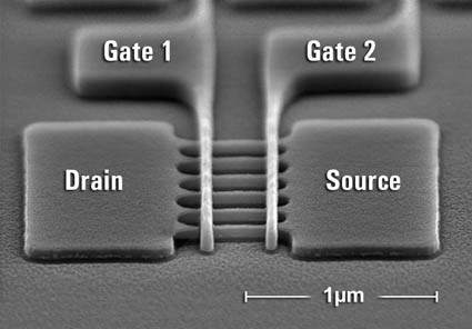
Munich (Germany) - Infineon today said that it has developed multi-gate FINFET transistors, often also described as 3D transistors that dramatically reduce the amount of leakage current. The chip company believes that portable devices built around 3D transistors technology could run about twice as long as products using traditional planar circuitry.
The potential of multi-gate transistors, which has been explored by firms such as IBM, TSMC, Infineon and Z-RAM developer Innovative Silicon, could emerge into a solution to keep control of power consumption in silicon chips that quickly scale into smaller structures while increase their performance at the same time. Infineon, which was among the first companies to present first details about 3D transistors about two years ago, now said that it has succeeded in building a complex circuitry using multi-gate FINFET (Fin Field Effect Transistor) transistors that could open the door to chips that use considerably less power than devices manufactured today.
The company developed a 65 nm chip, which contains "more than 3000 active transistors fabricated in three-dimensional multi-gate technology." First test have shown that multi-gate transistors are "just as powerful as today's mature technologies," Infineon said. However, the new approach consumes "as little as half as much energy for the same functionality," the company claims.
Much of the reduced power consumption can be attributed to the decrease of leakage current. Leakage current, a common problem in transistor technology, refers to "wasted" power at the transistor level that are caused by multiple effects, for example "source-to-drain leakage," which refers to electrons that are compelled by the doping element in the drain, even when the transistor state is supposed to be Off. As a result, even if transistors are inactive, they consume a certain amount of power. Scaling transistors typically increased the amount of leakage current; however, Intel, for example, was able to revert that effect with the introduction of 65 nm devices such as the Core Duo processor.
Infineon's multi-gate transistor
Infineon believes that 3D transistors can reduce leakage current dramatically. In today's press release, the company claims that the 3000-transistor test chip showed 10 times less leakage current than a single-transistor device. That factor will increase "significantly" in "32 nm devices and beyond," the firm stated. This effect alone could double the battery life of portable devices, according to Infineon.
Because the technology enables to build transistors "three-dimensionally" - as opposed to the planar transistors in production today - the space required to integrate a certain amount of transistors shrinks. According to Infineon, 65 nm multi-gate transistor architecture requires about 30% less two-dimensional space than single-gate technology with the same functions and performance.
Get Tom's Hardware's best news and in-depth reviews, straight to your inbox.
Infineon's multi-gate transistors are still deep in their research phase and will not be used in mass-production until 2012 or later, Infineon said. Looking at today's semiconductor roadmaps, 32 nm and 22 nm semiconductor structures will be business as usual until then.
In the microprocessor space, AMD could be using the technology through an investment in Z-RAM developer Innovative Silicon. Intel recently provided details about its own tri-gate transistor technology, which is expected to be available in 2009 for 32 nm processors and promises to use 35% less power than today's transistors.
Related content:
Tom's Hardware is the leading destination for hardcore computer enthusiasts. We cover everything from processors to 3D printers, single-board computers, SSDs and high-end gaming rigs, empowering readers to make the most of the tech they love, keep up on the latest developments and buy the right gear. Our staff has more than 100 years of combined experience covering news, solving tech problems and reviewing components and systems.


