VIA VT8188A: Details On Thermal Protection
This circuitry is used on the VIA reference board. The thermal protection is controlled by the Maxim chip.
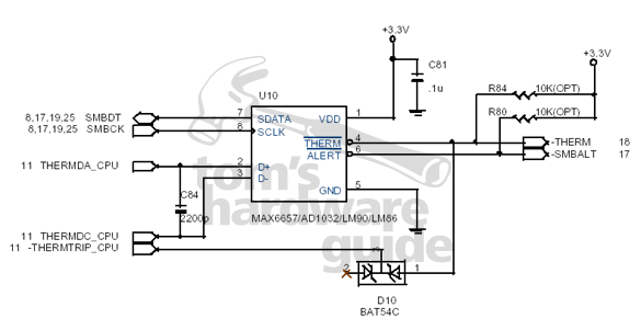
The following images show the reference material for manufacturing the VIA VT8188A boards. The interesting part is how the thermal diode is controlled: an external chip of the type 6657 from Maxim (AD1032, or LM90/LM86) takes over the overload protection of the K8 CPU. According to Maxim, the chip can detect temperatures between 60 and 100 degrees Celsius, where the test frequency is 16 Hz (16 test per second). The results of the first tests will show whether or not the CPU has additional internal protection. In any case, the logic of the Maxim chip can be avoided with the circuit signal "THERMTRIP_CPU." Just as with the Athlon XP, the motherboard is switched off through protection circuitry. The circuit diagram shows the fundamental structure.
Details On The Motherboard: Sockel 754 For The Hammer

A view of the Motherboard with Socket 754.
The Motherboard is the first board for the Socket 754 platform to arrive in the THG lab. It's based on the VIA K8T400M chipset and is equipped with the VIA VT8235 Southbridge. Three memory slots can be fitted with DDR333 at the most. An interesting feature is the integrated vacuum tube amplifier for 5.1 surround sound. Here, three tubes (satellite, center and stereo channels) are responsible for processing the analog signal. The following images give you a basic idea of how motherboards for the AMD Hammer are built.

The Northbridge of the K8T400M chipset.

The "Tube" in the board name refers to the vacuum tube amplifier.

The table for the Front Side Bus. Settings ranging from 100 MHz to 200 MHz are possible.

Underside: the contacts for the three tubes.

Underside of the Motherboard.

Detailed photo of the underside of the CPU socket. The short distances to the Northbridge and to the memory are clearly noticeable. The holes and fasteners of the clamp for the CPU cooler can also be seen.

The three tubes of the Motherboard with 5.1 technology.

The Southbridge VIUA VT8235: Ultra-DMA/133 and USB 2.0 are integrated.