Researchers Create World's Smallest Semiconductor Laser
Researchers at The University of Texas at Austin have come closer to a all-optics chip.
Their new laser, claimed to be the smallest in the world, is so small that it cannot be seen with the naked eye.
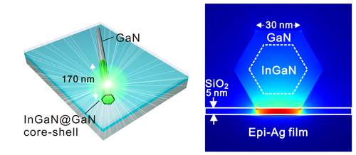
The laser was built using a 30 nm gallium nitride nanorod that is partially filled with indium gallium nitride. The nanorod is placed on a 5 nm thin silicon dioxide gap layer that is sandwiched between the nanorod and an "atomically smooth" 28 nm silver film. Chih-Kang “Ken” Shih, professor of physics at The University of Texas at Austin, said that “atomic smoothness is key to building photonic devices that don’t scatter and lose plasmons, which are waves of electrons that can be used to move large amounts of data." Shih said that he has been experimenting and improving the material for more than 15 years.
So far, the size and performance of photonic devices have been restricted by what is known as the three-dimensional optical diffraction limit, which was described by two German researchers in a paper published in Laser & Photonics Reviews earlier this year. However, their new, green light emitting laser operates "well below" the 3D diffraction limit. Shih and his team believe that their tiny laser will have a huge impact on photonic chip development and promote the development of chips that are fully photonic and integrate “on-chip” communication systems.
Article continues belowContact Us for News Tips, Corrections and Feedback
Get Tom's Hardware's best news and in-depth reviews, straight to your inbox.

Douglas Perry was a freelance writer for Tom's Hardware covering semiconductors, storage technology, quantum computing, and processor power delivery. He has authored several books and is currently an editor for The Oregonian/OregonLive.
-
Chainzsaw With this small laser - does this mean optical media can be further enhanced by more data being able to fit in the same space?Reply
This seems like it would be great for future processors/RAM for communications - since light does not have limitations copper has. -
phatboe ChainzsawWith this small laser - does this mean optical media can be further enhanced by more data being able to fit in the same space?Doubtful since it still emits green light.Reply -
jkflipflop98 ChainzsawWith this small laser - does this mean optical media can be further enhanced by more data being able to fit in the same space?This seems like it would be great for future processors/RAM for communications - since light does not have limitations copper has.Reply
Nope, what this means is that Thunderbolt controller chips are about to get really cheap. This can theoretically be used to replace the waveguide circuitry on motherboards and the copper interconnect layers in a processor. . . but that also means one needs to built a optical transmission/reception device at either end hence completely nullifying the whole purpose of simplifying the circuit with a laser in the first place.
-
onichikun Also it isnt that easy to grow GaN on silicon substrates, since it puts quite a bit of stress on the silicon lattice its grown on. It would be nice to have optical transmission on chip, but this technology is going to be hard to integrate into todays fab processes.Reply -
A Bad Day ChainzsawThis seems like it would be great for future processors/RAM for communications - since light does not have limitations copper has.Reply
Although optics would most likely have superior latency and bandwidth, data deteriorate faster over very short distances (like less than a few centimeters) on optics than copper. -
11796pcs ReplyThe laser was built using a 30 nm gallium nitride nanorod that is partially filled with indium gallium nitride.
Sorry Tom's, you lost me there. -
fazers_on_stun IIRC copper conducts electrical signals at around 2/3rds the speed of light in a vacuum - so that's 2 x 10^8 meters per second as opposed to 3 x 10^8 m/s - still pretty fast in my book :P.Reply
From what I've read, the big problem in optical processing is switching or steering the light signals into the correct logic (directional) path without having to transduce it to an electrical signal, gating it to the appropriate output, and then transducing it back to an optical signal. If that can be done cheaply and efficiently, then we're talking processing speeds in the terahertz range as opposed to a few GHz as with electrical CPUs or GPUs. Basically optical switching uses input optical signals to gate or switch optical output signals, requiring much less power and having switching times orders of magnitude less than their CMOS logic gate counterparts.
However this seems to be yet another 'promising' technology always stuck in the lab, sorta like those infamous carbon nanotube enhanced batteries that DailyTech and THG used to go on and on about for years. Still waiting on that 48-hour battery that seemed to be "right around the corner" back in 2008, BTW... :P
