Intel’s X-Lab: Tomorrow’s Network Happens Here
Get Tom's Hardware's best news and in-depth reviews, straight to your inbox.
You are now subscribed
Your newsletter sign-up was successful
Power Delivery Testing
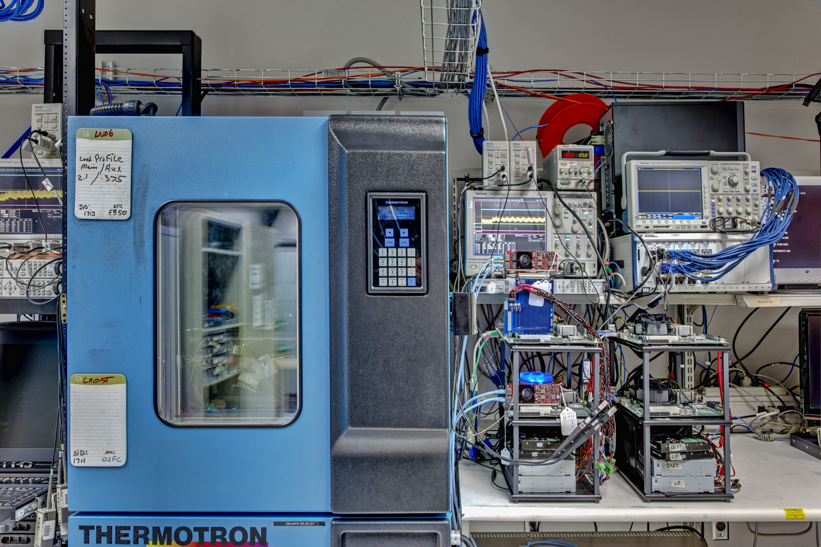
Moving on. One can’t help but admire the array of different homegrown systems scattered across Intel’s labs. Chassis side panels seem scorned, and not much attention gets paid to PC cable management since there are simply too many mods and a semi-constant need to change equipment. It’s all function over form.
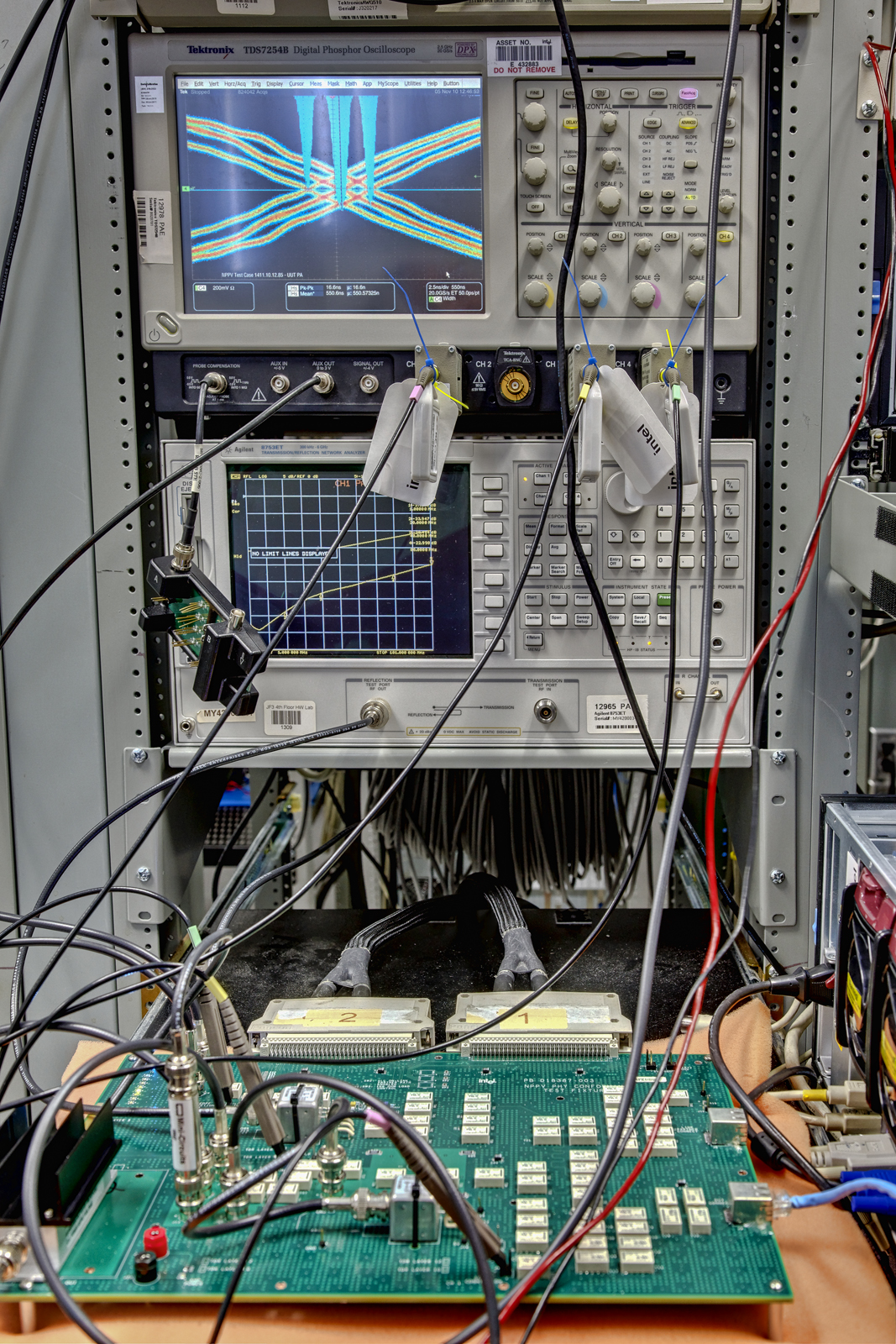
Take the above setup as an example. It’s a collection of gear designed to test the power delivery network of Intel networking silicon. Engineers look to characterize the chip’s power consumption, power quality, and efficiency. With the inevitable rise of 10GbE products, power consumption and efficient power delivery will only become increasingly important.
“10GBASE-T in particular has provided a new challenge in that, with these early silicon generations at least, we no longer have the power margins of 1GbE,” noted Pete. Some may recall that early 1 Gb Ethernet chips were quite power-hungry, as well. “Our power delivery testing ensures that our 10GbE products adhere to PCIe specification limits as well as meeting customer expectations.”
Article continues belowHot Technology
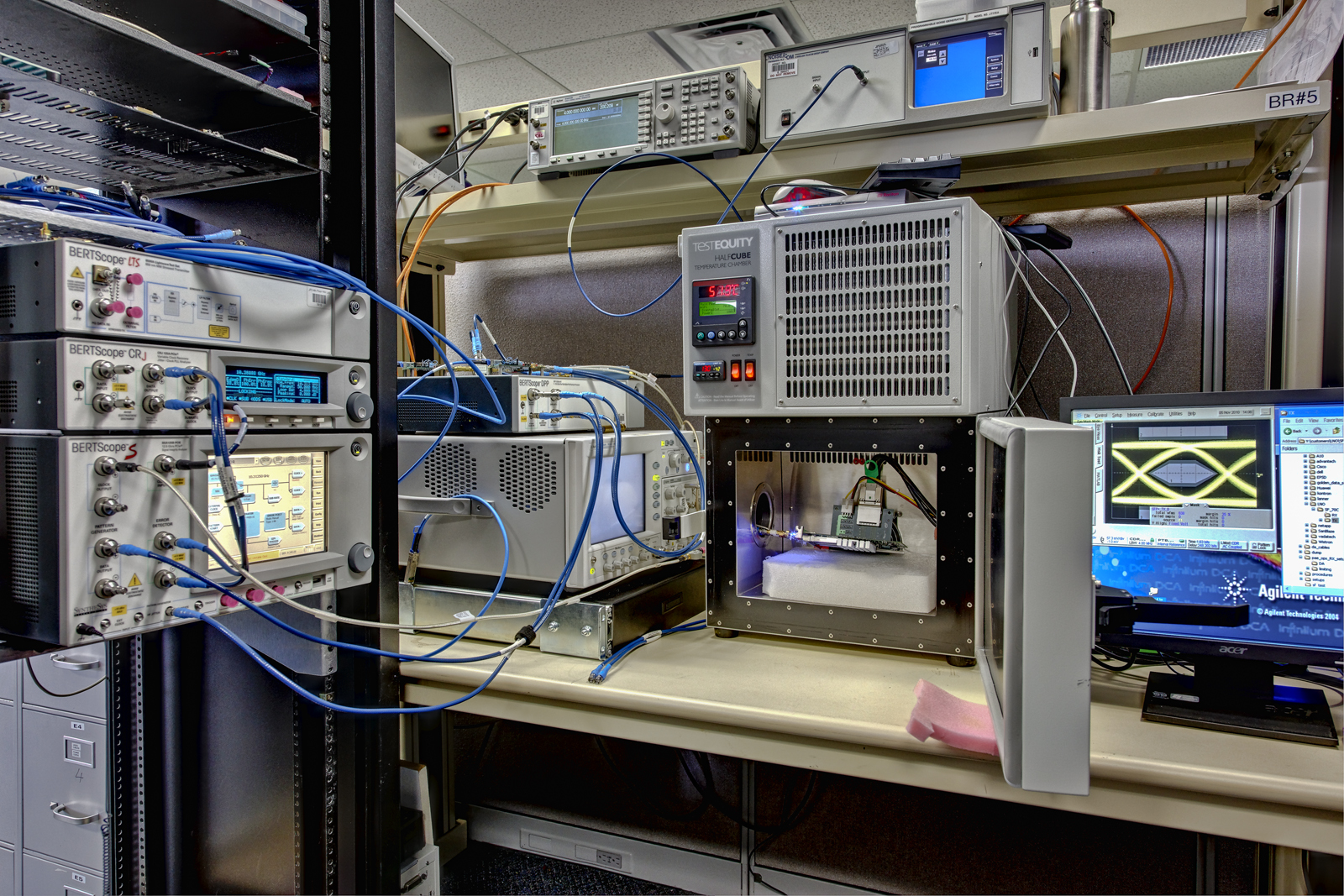
For systems running at high temperatures, Intel needed to create an isolated environment in which engineers could drive the temperature of the card independently of the system. The other PC components are fairly irrelevant. They’re all off-the-shelf and qualified elsewhere. In this case, Intel just wanted to focus on the NIC.
Engineers created a homebrew enclosure in which compressed air gets piped in and exhausted out the back. The very first design was made from cardboard, but then progressed to Plexiglas. Today, the design is widely used across Intel’s labs.
The in-progress test shown here has this NIC baking at 57.8˚C during operation.
Helping Out Buyers
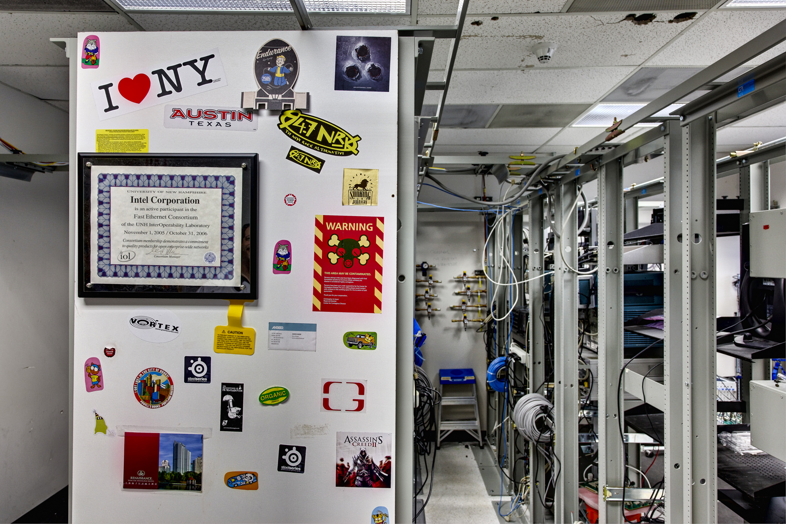
I’m learning that, in the world of R&D and engineering, there’s a fine line dividing the clean room from the garage. This little space is just big enough for two rack rows, but it’s where Intel does the bulk of its validation and troubleshooting work for OEMs—original equipment manufacturers that purchase Intel’s networking silicon for use in their own systems. You can see holes in the ceiling where prior infrastructure once ran. The cramped room is relatively loud from the thrumming of system fans. In this photo, you can see the end cap, directly facing the room’s one entrance, where staff display their assortment of radio, gaming, and other bumper stickers. A certificate from the University of New Hampshire’s InterOperability Laboratory, something of a Mecca in the Ethernet validation world, dominates the eclectic collection.
Get Tom's Hardware's best news and in-depth reviews, straight to your inbox.
Patching And Problems
Once silicon and NIC reference designs are finalized, Intel will send the products to OEMs, who in turn create their systems and return early samples back to Intel for analysis. Intel then compares those OEM products against proven reference board results. If the OEM data looks worse, an Intel technical marketing engineer will go over the OEM’s schematics and work to help the manufacturers improve their quality. Sometimes, engineers are even called on to do failure analysis in the field.
“I’m doing a laptop project now where there may be a cold solder joint problem,” said Intel’s Matt Wonson. “Like you desolder and resolder the network silicon, and all the problems go away.”
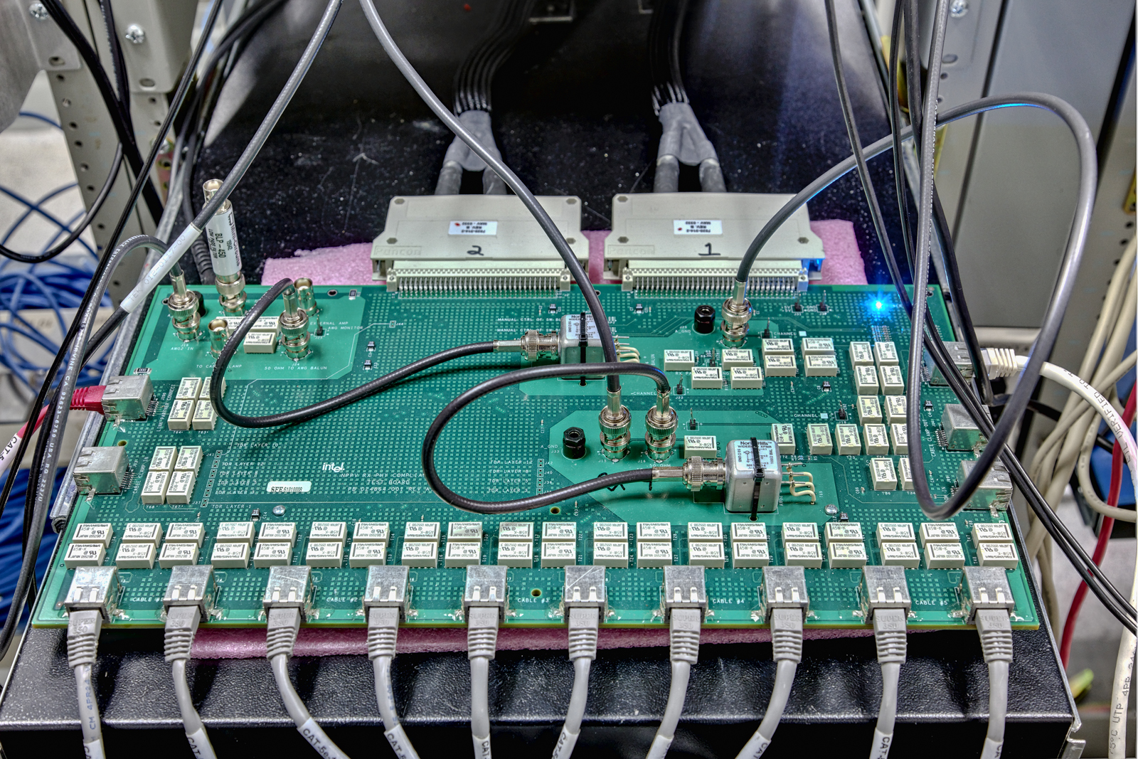
Matt works in new products testing, customer designs, and troubleshooting. The testing and troubleshooting work done here looks somewhat familiar to that done in the X-Lab. For example, the station shown above is for doing bit error rate testing. Techs can use relays to patch cables for lengths up to 160 meters. “As the test runs,” said Matt, “it finishes one cable length, then uses the relays to create a sort of virtual cable.”
Part Of The Bargain
“This station over here is doing some transmit testing,” continued Matt. “It’s a little more complex, with more stuff on it. We’ll have the oscilloscope hooked up to that, measuring. We’ve got different cable models and stuff on the board, so as each test runs, the board switches to the appropriate load for that test. The way that the racks work is we’ve got a controller PC with a GPIB controller card in it that talks to all of the different instruments. So when it’s getting a run—say you have to have a certain capture length—the controller PC tells the scope to capture this long of a record, maybe along with some screen grabs. It’s got pass/fail criteria, what’s marginal, what was actually measured. Right now, I’ve got these Powerville 4-port, GigE, no bridge chip network cards that do Energy Efficient Ethernet. That’s one of the big things in power right now.”
Intel doesn’t charge for this support. Anybody who buys Intel silicon can get these test results for their product. The University of New Hampshire has its Interoperability Test program, and it’s the most renowned lab in this space, but, according to my tour hosts, the consortium fees can add up fast for a low-margin manufacturer.
“So we’ll provide all that support plus review your design and suggest what components to use on magnetics or resistors or whatever,” said Matt. “We may not always be the lowest-cost solution, but we bring a lot to the table.”
Thinking Inside The Box
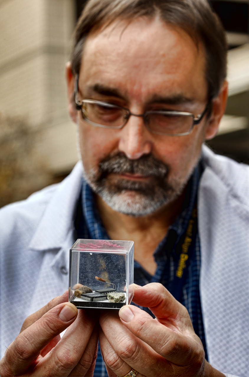
On the odds-and-ends shelf near the X-Lab’s door, there’s a small, clear box containing a palmful of trinkets. It reminds me of a similar jar of junk I have in my garage—some random memorabilia from my childhood. The box belongs to Pete, and I wondered if its contents might somehow illuminate his personality and perhaps his work at Intel.
“This is my way of remembering the moments,” said Pete, gazing into the box. “In my prior career, I was actually a failure analysis engineer. My job was to find problems with chips. Someone found this little bugaboo thing, a little digital IC thing with a capacitor. It looks kind of bug-ish. Over the years, I’ve thrown in different chips that have caused me great pain and excitement. And it was a place I could throw my chunk of trinitite. It changes over the years, but it’s been pretty stable because Intel is pretty good!”
Trinitite is fused glass from the first atomic bomb test in 1945. I have to assume that, for Pete, the shard represents a landmark shift in technology and its impact on the world.
“The most outstanding of these chips is probably this little motion control chip from my prior job,” he added. “We were starting to do some analysis on it, and the top literally fell right off in the middle of testing. That’s not something you want to have happen to your silicon.”
Our Token Ring Of Techs
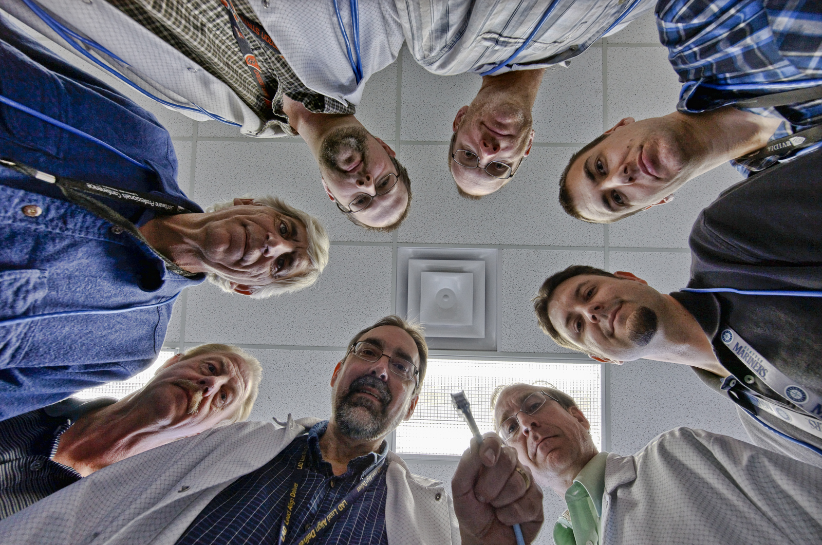
What’s a good tour without a group shot? Pete, surrounded here by several of his teammates, holds some CAT6a cable and prepares to plug back into his day job, having finished shepherding us around his labs. Wrapping up, it’s clear to me how much we take for granted. We plug in our network connections, they work, we’re happy, end of story. Only it’s not. There’s a mind-boggling amount of work, ingenuity, and expense (the X-Lab room alone houses over $5 million in test gear) that goes into making your network connection possible and reliable.
Pete and his team are a vital part of making your data connection a reality. And when you get faster feeds tomorrow, when 10GbE finally lands on your desktop in the next few years, and when you can transfer terabytes in the time it now takes you to send gigabytes, maybe give a silent nod to the X-Lab crew and remember all the years of work that made your connection possible.
-
super_tycoon dogman_1234Anyone else notice the Guy Fawkes mask in the background?Reply
It's existence is noted in the text for pic3, though I can only wonder why he has it. Is it good taste to associate yourself with 4chan and anon nowadays? -
gmoney86 I am not sure if I ever saw the sign to the X-Lab when working at Jones Farm, but I did always wonder what went on in the labs that were similar to it. They kind of looked like IT work rooms to me, though it makes sense to have a need for oscilloscopes, soldering irons, networking tools, etc. for certain R&D projects.Reply -
scook9 Awesome article, I just finished me BSEE degree and now work in an network company where I help engineer servers so this is right up my alley!Reply -
This all started in 1990 with the creation of EtherExpress 16 by a handful of people led by a visionary leader, Steve Kassel.Reply
-
williamvw super_tycoonIt's existence is noted in the text for pic3, though I can only wonder why he has it. Is it good taste to associate yourself with 4chan and anon nowadays?My guess is that it was just a fun-looking mask someone had brought to the lab, perhaps because they also enjoyed "V for Vendetta." (I did!) I'd wager that the X-Lab crew had no idea of the mask's fleeting association with 4chan's anti-Scientology protests, much less the religious motivations behind Fawkes's attempted regicide. Let's not accuse good people without cause.Reply -
chovav Excellent article Tom (Willam actually). Nice reading, informative and geeky, just the way I like it. Amazing to see that they transfer 76TB in just one test (500,000,000*1518*100). Good job!Reply -
williamvw chovavExcellent article Tom (Willam actually). Nice reading, informative and geeky, just the way I like it. Amazing to see that they transfer 76TB in just one test (500,000,000*1518*100). Good job!Yeah, I was stunned. I honestly expected some automated tests, maybe a few guys with scopes taking occasional signal readings -- NOTHING like what I saw. I'd assumed that a technology as old as Ethernet was pretty much a done deal and didn't require much hand holding at this point. I couldn't have been more wrong.Reply
