12 Socket 370 Motherboards using VIA's Apollo Pro 133A
Back To The Roots - Continued
Intel had to find a compromise. As they did not want to relocate the L2 cache back onto the motherboard and integrating it into the CPU die was not possible at that time, the Slot-1 was introduced. A little PCB was designed to carry the CPU and the additional L2-cache chips, which were now allowed to run at only half the processor clock.
The original Pentium II Klamath was soon replaced by the Deschutes, which was also the first CPU designed for 100 MHz FSB. Last year, Intel introduced the Pentium III (with Katmai core), featuring their new Streaming SIMD Extensions (SSE). Only a few months later, they introduced the Coppermine core, which finally came with on-die L2-cache running at core clock.
AMD is currently undertaking the same move from a cartridge solution with extra L2-cache chips running at 1/3 - 1/2 of the core clock to a socket solution for the upcoming Thunderbird core, which also hosts full speed L2-cache on the processor die.
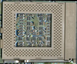
This photo shows the Socket 7. It was first used for the second-generation Pentium processors (75 MHz and above) and later for Intel's Pentium MMX CPUs (up to 233 MHz). AMD has also been making use of Socket 7 for their K6 processor family (K6, K6-2, K6-III). Cyrix/IBM sold low end CPUs (6x86, 6x86MX) for this socket.
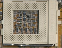
That's the socket you need for all Celeron and FC-PGA Pentium III CPUs.
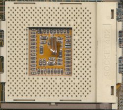
This photo shows AMD's new Socket A, which will be required for the new Thunderbird CPU.
Get Tom's Hardware's best news and in-depth reviews, straight to your inbox.

Patrick Schmid was the editor-in-chief for Tom's Hardware from 2005 to 2006. He wrote numerous articles on a wide range of hardware topics, including storage, CPUs, and system builds.


