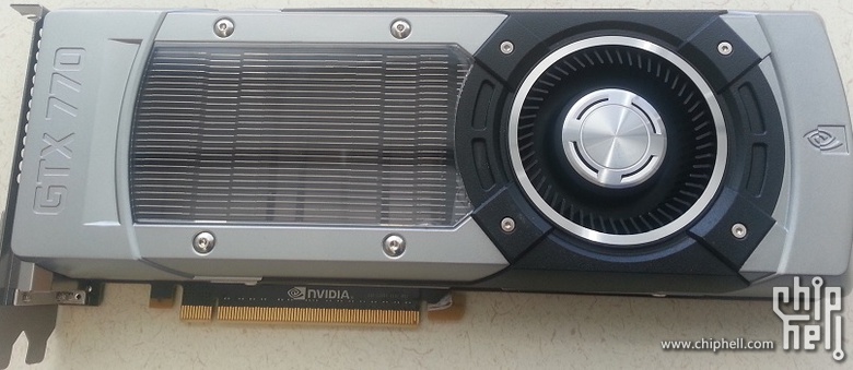
Report: GTX 770 Spotted Again, Specifications Confirmed
A new image of the GTX 770 has been leaked by the folks over at Chiphell.
Because a number of people were doubtful about the validity of the previous images of the GTX 770, Chiphell has released yet another image. In the meantime, there's also been more talk of the specifications.
The graphics card will apparently pack the GK104 GPU with eight of the SMX units enabled. This would give the card a total of 1536 enabled CUDA cores, 128 TMUs, and 32 ROPs. The base clock would be 950 MHz, with the boost clock set at 980 MHz. The card would also have only 2 GB of GDDR5 memory, which would run at an effective speed of 6.00 GHz over a 256-bit memory bus, letting it pump out 192 GB/s of bandwidth. This makes the GPU and memory parts of the card almost identical to the GTX 680.
What appears to be different is the PCB design. Apparently, the card has a lot more overclocking headroom due to a standard TDP of 250 W (vs. the 195 W of the GTX 680). The default voltage would also be above 1.3 V. The card would be fueled by a 6-pin and 8-pin PCIe power connector setup. The PCB is reportedly much more similar to the design of the GTX Titan rather than the GTX 680, although this particular sample could be an engineering sample.
Article continues belowIt also appears that the card will launch on May 30, 2013.
| Header Cell - Column 0 | GPU | CUDA Cores | TMUs | ROPs | Memory | Memory Interface |
|---|---|---|---|---|---|---|
| GTX 780 | GK110 | 2,496 | 208 | 40 | 3 GB | 320-bit |
| GTX 770 | GK104-425 | 1,536 | 128 | 32 | 2 GB | 256-bit |
| GTX 760 Ti | GK104-225 | 1,344 | 112 | 32 | 2 GB | 256-bit |
Get Tom's Hardware's best news and in-depth reviews, straight to your inbox.
Niels Broekhuijsen is a Contributing Writer for Tom's Hardware US. He reviews cases, water cooling and pc builds.
-
vmem there're also rumors online that you can BIOS flash a 680 into a 770 due to largely similar specs and practically the same die...Reply
either way, it's sounding more and more like this is a publicity stunt for Nvidia and their attempt to get even more money out of kepler, rather than being forced to drop prices as the current series age... -
CaedenV I am surprised at the limit of 2GB of ram on mainstream cards. My last upgrade was to the GTX570 with 1.2GB of ram. More than enough processing power for my needs (until I get a higher res monitor some day), but I have already capped out the ram on games like Skyrim.Reply
With next gen games coming out this year, and consoles putting much more emphases on memory capability compared to previous generation upgrades, I would imagine games coming out over the next 2 years to absolutely balloon on GPU ram requirements. And this will be doubbly true for PC gaming where better textures are typically the bonus to buying into the ecosystem. My next upgrade may not need that much GPU power, but I am thinking a minimum of at least 3-4GB of ram so that I do not get burnt again on capacity issues. -
jk_ventolero Meh, no matter. I won't be owning any of these any time soon. I just clicked so I can drool over the image. LOLReply
I might still get an AMD card for my next upgrade. :) -
tigger888 turns out that 770 is a reflashed 680. google search it. :D you get a 5% performance boost.Reply -
hapkido So they're releasing slightly modified versions of their existing cards as a new series? No wonder AMD is skipping a numbering gen. Bring on HD 9xxx later this year and maybe Nvidia will answer with GTX 8xx shortly after.Reply
I really can't afford to upgrade, but I'd like to get another pricewar going on new hardware so I can make an excuse to. -
JJ1217 Damn. Those shrouds look sexy. Only reason I want one. I hope the 8XX series has those sexy shrouds the titan has.Reply -
iamtheking123 Owning a 680 Lightning right now, I can tell you "above 1.3V", which I run at, uses a TON of power. Each of my cards uses 350W from the wall under full load, and I had to buy a new power supply after I was exceeding one of the 12V rails in my old PSU (30A limit).Reply -
Novuake If they implement GPU Boost 2.0 instead of 1.0 on all these cards, I would consider it, if not, screw it. Stick with AMD till Nvidia impresses me again.Reply -
Novuake If they implement GPU Boost 2.0 instead of 1.0 on all these cards, I would consider it, if not, screw it. Stick with AMD till Nvidia impresses me again.Reply -
Novuake If they implement GPU Boost 2.0 instead of 1.0 on all these cards, I would consider it, if not, screw it. Stick with AMD till Nvidia impresses me again.Reply

