Samsung Mass Producing 3D Vertical NAND Flash
A new era in flash NAND has begun.
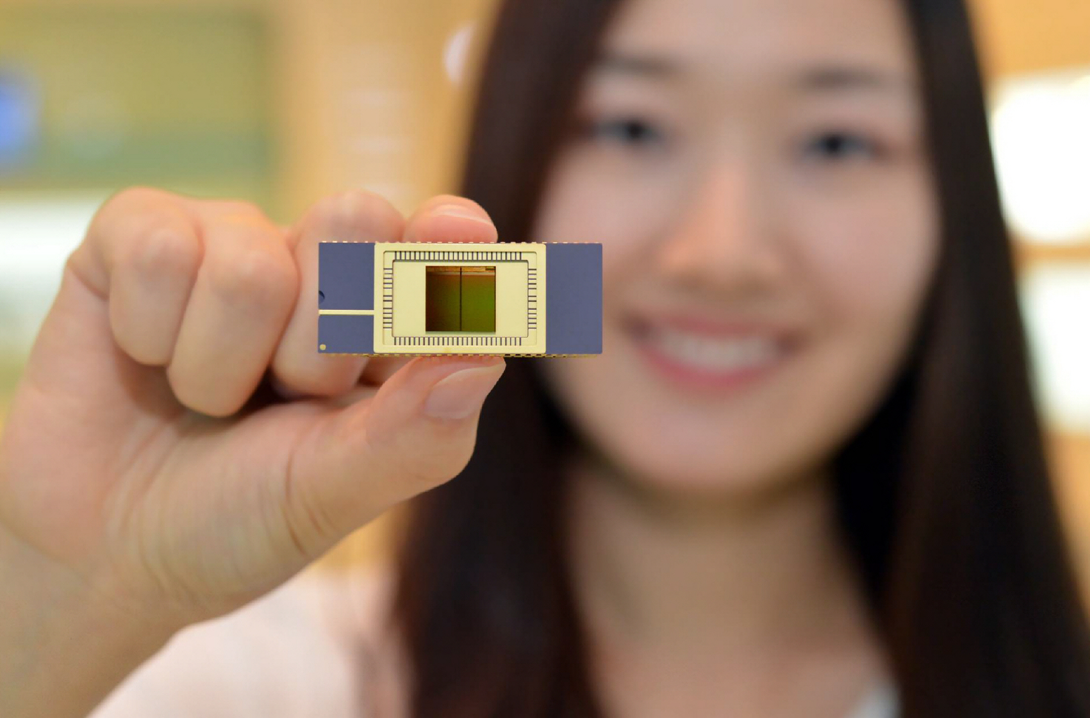
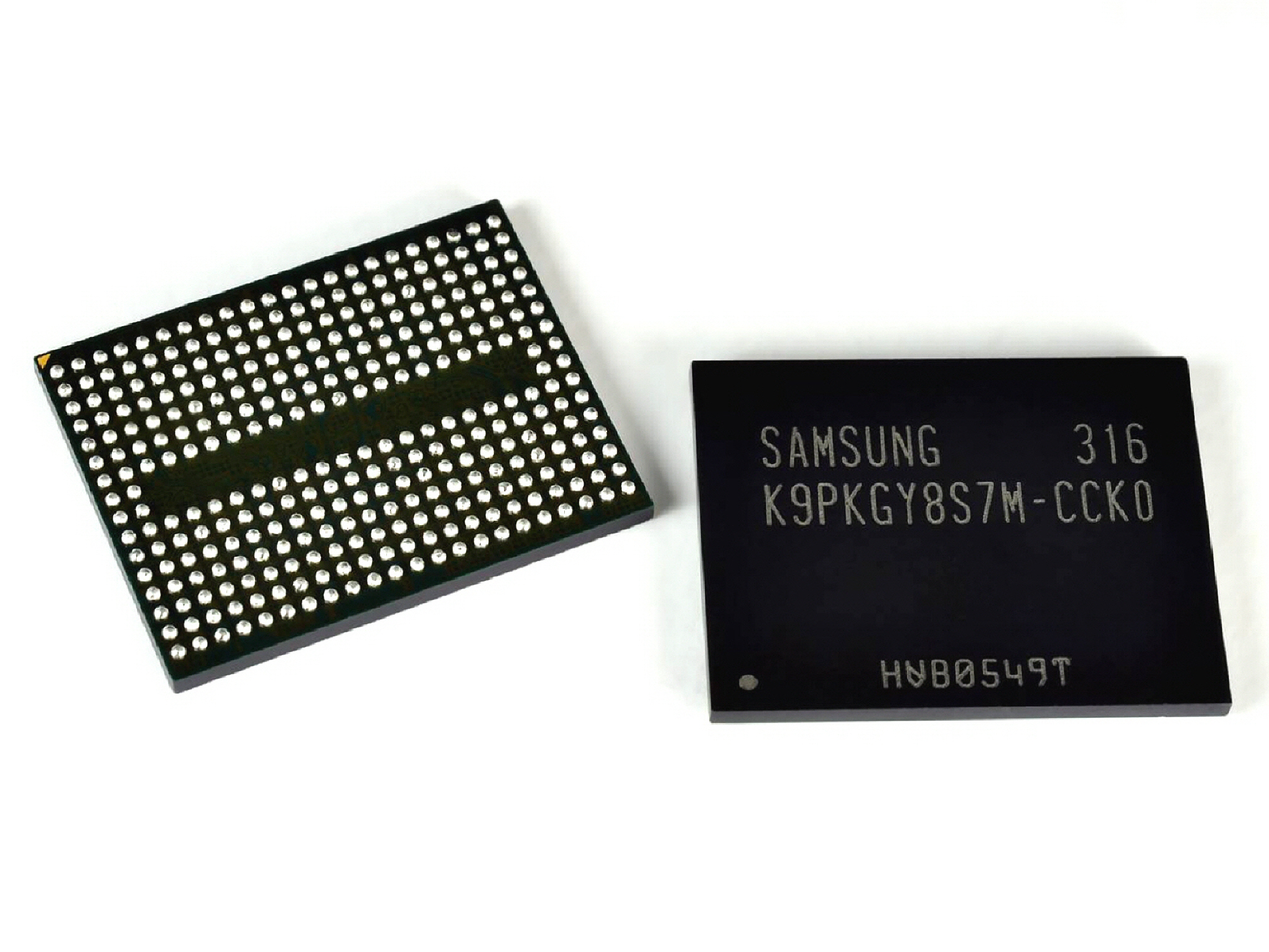
Samsung Electronics said on Monday that it is now mass producing the industry's first 3D Vertical NAND (V-NAND) flash memory, offering a 128 gigabit (Gb) density in a single chip.
According to Samsung, V-NAND breaks away from the floating gate-based planar structure that has been used in conventional memory over the past 40 years. It does this by utilizing the company’s proprietary vertical cell structure based on 3D Charge Trap Flash (CTF) technology, and vertical interconnect process technology to link the 3D cell array. By applying both of these technologies, it's able to provide over twice the scaling of 20nm-class planar NAND flash.
With manufacturing process shrinking down to 10 nm levels and beyond, there has been growing concern about a limit to scalability due to cell-to-cell interference that causes a trade-off in the reliability of NAND flash products. The new V-NAND solves this problem by vertically stacking planar cells, a method that was finally achieved after revamping Samsung's CTF architecture which went into development back in 2006.
Article continues below"In Samsung’s CTF-based NAND flash architecture, an electric charge is temporarily placed in a holding chamber of the non-conductive layer of flash that is composed of silicon nitride (SiN), instead of using a floating gate to prevent interference between neighboring cells," the company explained. "By making this CTF layer three-dimensional, the reliability and speed of the NAND memory have improved sharply."
Samsung said its vertical interconnect process technology can stack as many as 24 cell layers vertically, using a special etching technology that connects the layers electronically by punching holes from the highest layer to the bottom. Thus by using a vertical structure, higher density NAND products can be achieved by increasing the 3D cell layers without having to continue planar scaling.
Samsung said the 3D V-NAND shows an increase of a minimum of 2X to a maximum 10X higher reliability, and twice the write performance over conventional 10nm-class floating gate NAND flash memory.
"The new 3D V-NAND flash technology is the result of our employees’ years of efforts to push beyond conventional ways of thinking and pursue much more innovative approaches in overcoming limitations in the design of memory semiconductor technology," said Jeong-Hyuk Choi, senior vice president, flash product & technology, Samsung Electronics. "Following the world’s first mass production of 3D Vertical NAND, we will continue to introduce 3D V-NAND products with improved performance and higher density, which will contribute to further growth of the global memory industry."
Get Tom's Hardware's best news and in-depth reviews, straight to your inbox.
Nearly ten years of research was dumped into 3D Vertical NAND, the company said, and it now has more than 300 patent-pending 3D memory technologies worldwide. The new 3D V-NAND will be used for a wide range of consumer electronics and enterprise applications, including embedded NAND storage and solid state drives (SSDs).

Kevin Parrish has over a decade of experience as a writer, editor, and product tester. His work focused on computer hardware, networking equipment, smartphones, tablets, gaming consoles, and other internet-connected devices. His work has appeared in Tom's Hardware, Tom's Guide, Maximum PC, Digital Trends, Android Authority, How-To Geek, Lifewire, and others.
-
CaedenV Now this is exciting news! Back in the '90s when die shrinks were becoming a popular way to bring performance improvements everyone was talking about how there is a limit to how small you can really go (back at the time they thought the limit was ~20nm or so). But the thought was that after the end of the die shrinks then we would either have to make changes by building 3D structures, layered structures, or maybe abandon the way we view tech and move to 'something else'. I was a kid at the time, and so now as an adult I have a strange fascination about this time we are entering where there is less and less importance to die shrinks anymore.Reply
I think that for storage this is going to be a huge thing, especially for portable storage so that we can hopefully start getting 240GB+ of storage on phones and 1TB+ on tablets. But CPUs and GPUs are going to have some serious challenges moving to this kind of tech. Not only are the structures a whole lot more complicated, but they also produce a bunch of heat. I think that Intel was really hoping that things like Knight's Corner and the 'many core' designs would take off because each individual core would be much simpler, give off much less heat, and workloads could be distributed in a way so that once a core got warm then the load could move to a different core so that the entire unit would stay relatively cool. If they could accomplish that then each core could fit perpendicular to a back-plane, making for an insanely dense processing solution. But the fact of the matter is that normal workloads only take 1-2 cores and rarely up to 4, so this many core design does not work for most end users. To have a truly 3D CPU or GPU on current technology would just put out way too much heat to be practical yet, but I am sure they will think of something before too long. I mean, they really have to. -
JPNpower Intel 3d tech now in storage. Surprised that Intel didn't do this first for their ssd. They've sold the tech since ivyReply -
Giovanni-L A big round of applause. I'm getting sick of all developers giving ALL attention to the freaking software and none at all to hardware... I'm a hardware guy. I create tech designs as a hobby. Now i'm proud of Samsung, and i'm also proud of owning a Galaxy Note 2 5.5" smartphone. GO SAMSUNG, GO!!!Reply -
back_by_demand Prepare for 10Tb SSDs - this is real innovation, NOT rounded corners - in light of recent events if I were Samsung I would keep this tech and not license it and if Apple come knocking to buy some tell them to go fu@k themselves.Reply -
mavikt You've just got to love REAL progress! Seems like SSDs could displace HDDs in a not too distant future.Reply
I hope they haven't been cuting any corners, though it's unlikely they'll be getting any patents on rounded corners, ha.
I'm on vaccation, typing this on à borrowed "touch" pad. I miss My keyboard!!! -
alidan Reply11300584 said:Now this is exciting news! Back in the '90s when die shrinks were becoming a popular way to bring performance improvements everyone was talking about how there is a limit to how small you can really go (back at the time they thought the limit was ~20nm or so). But the thought was that after the end of the die shrinks then we would either have to make changes by building 3D structures, layered structures, or maybe abandon the way we view tech and move to 'something else'. I was a kid at the time, and so now as an adult I have a strange fascination about this time we are entering where there is less and less importance to die shrinks anymore.
I think that for storage this is going to be a huge thing, especially for portable storage so that we can hopefully start getting 240GB+ of storage on phones and 1TB+ on tablets. But CPUs and GPUs are going to have some serious challenges moving to this kind of tech. Not only are the structures a whole lot more complicated, but they also produce a bunch of heat. I think that Intel was really hoping that things like Knight's Corner and the 'many core' designs would take off because each individual core would be much simpler, give off much less heat, and workloads could be distributed in a way so that once a core got warm then the load could move to a different core so that the entire unit would stay relatively cool. If they could accomplish that then each core could fit perpendicular to a back-plane, making for an insanely dense processing solution. But the fact of the matter is that normal workloads only take 1-2 cores and rarely up to 4, so this many core design does not work for most end users. To have a truly 3D CPU or GPU on current technology would just put out way too much heat to be practical yet, but I am sure they will think of something before too long. I mean, they really have to.
11303671 said:Prepare for 10Tb SSDs - this is real innovation, NOT rounded corners - in light of recent events if I were Samsung I would keep this tech and not license it and if Apple come knocking to buy some tell them to go fu@k themselves.
brute force is going to die at some point, thats what single core applications are basicly, they require a faster cpu to run faster no matter how many cores there are.
amd has a solution, and is in every new console, along with the pc, multi core, and multithreaded is going to work its way into the games second, first was pro programs, and it may trickel down to consumer programs.
i can honestly see a day when there is one power house cpu (something that can run single core applications really really fast) and the rest of the cpu is made up of smaller cores that work together to distribute the load. the fast single will require the heat sync, but the small distributed may be possibly to cool passively while working faster than what we have now.
but a new cooling solution would probably be the best way to go.
graphene to my knowledge can handle the 50-200ghz speed on air cooling
just imagine that at 3-5ghz, but with 40-120 cores stacked 3d.
and it may not be initially, but the 3d process will fall under frand., not giving samsung the ability to tell apple to eff off. -
JPNpower Brute force AND multi parallel will all eventually taper off in favor of efficiency, but the future is bright. Brute force for Processors have mostly been saturated, forcing cool innovation.Reply
And why you mention Samsung and Apple? 3D tech is being developed and tested in super wide areas by many companies. Also, 3D can mean stacking, but not in the near future. Think more along the lines of Ivy/Haswell 3D transistors. Yes, high density parallel stuff will happen anyways, but not how you imagine it.

