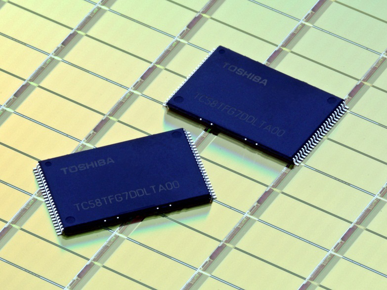
Toshiba, SanDisk Dip Into 15nm Process Technology
On Wednesday, Toshiba announced the launch of its 15nm process technology. This tech will be applied to 2-bit-per-cell 128 gigabit (16 gigabytes) NAND Flash memories, replacing second generation 19nm process technology. Mass production with the new technology will start at the end of April at Toshiba's Fab 5 Yokkaichi Operations.
According to Toshiba, chips based on the new processing technology will have improved peripheral circuitry technology. They will also achieve the same write speed as chips formed with 19nm process technology, but boost the data transfer rate to 533 megabits per second, 1.3 times faster, by employing a high speed interface.
"Toshiba is now applying the 15nm process technology 3-bit-per-cell chips, and aims to start mass production in the first quarter of this fiscal year, to June 2014," Toshiba said in a statement. "The company will develop controllers for embedded NAND flash memory in parallel and introduce 3-bit-per-cell products for smartphones and tablets, and will subsequently extend application to notebook PCs by developing a controller compliant with solid state drives (SSD)."
In a separate announcement, SanDisk reports that the technology will be available labeled as its 1Znm process node. The 15nm technology will ramp on both 2-bit-per-cell (X2) and 3-bit-per-cell (X3) NAND flash memory architectures, with production ramp to begin in the second half of 2014.
"We are thrilled to continue our technology leadership with the industry's most advanced flash memory process node, enabling us to deliver the world's smallest and most cost effective 128 gigabit chips," said Dr. Siva Sivaram, senior vice president, memory technology, SanDisk. "We are delighted that these new chips will allow us to further differentiate and expand our portfolio of NAND flash solutions."
The company reports that its All-Bit-Line (ABL) architecture contains proprietary programming algorithms and multi-level data storage management schemes, which is implemented in the 1Z technology to deliver NAND flash solutions "with no sacrifice in memory performance or reliability." The 1Z technology will be utilized across a broad range of products, the company reveals, including memory cards and enterprise SSDs.
Follow us @tomshardware, on Facebook and on Google+.
Get Tom's Hardware's best news and in-depth reviews, straight to your inbox.

Kevin Parrish has over a decade of experience as a writer, editor, and product tester. His work focused on computer hardware, networking equipment, smartphones, tablets, gaming consoles, and other internet-connected devices. His work has appeared in Tom's Hardware, Tom's Guide, Maximum PC, Digital Trends, Android Authority, How-To Geek, Lifewire, and others.
-
razor512 I can see the tech support complaints now (from toshiba's point of view). (HI tech support, I just got my new smartphone, and after taking a picture, all other writes either fail or end up corruptedReply
CSR: well you wrote over 2MB of data to your device, the NAND is as good as dead. If you would like, you can contact our supplier and order a case of 10,000 NAND BGA's and also this reflow solder station, and replace the NAND and reprogram the device using JTAG each time you need to take a new photo.
Customer: that sounds great! I will also order a gas generator so that I can take the solder station with me and reflow while on the go! -
BranFlake5 ReplyI can see the tech support complaints now (from toshiba's point of view). (HI tech support, I just got my new smartphone, and after taking a picture, all other writes either fail or end up corrupted
CSR: well you wrote over 2MB of data to your device, the NAND is as good as dead. If you would like, you can contact our supplier and order a case of 10,000 NAND BGA's and also this reflow solder station, and replace the NAND and reprogram the device using JTAG each time you need to take a new photo.
Customer: that sounds great! I will also order a gas generator so that I can take the solder station with me and reflow while on the go!
Yeah, Why are manufactures driving down flash die size? It hurts longevity, why bother?
