 Join Tom’s Hardware today


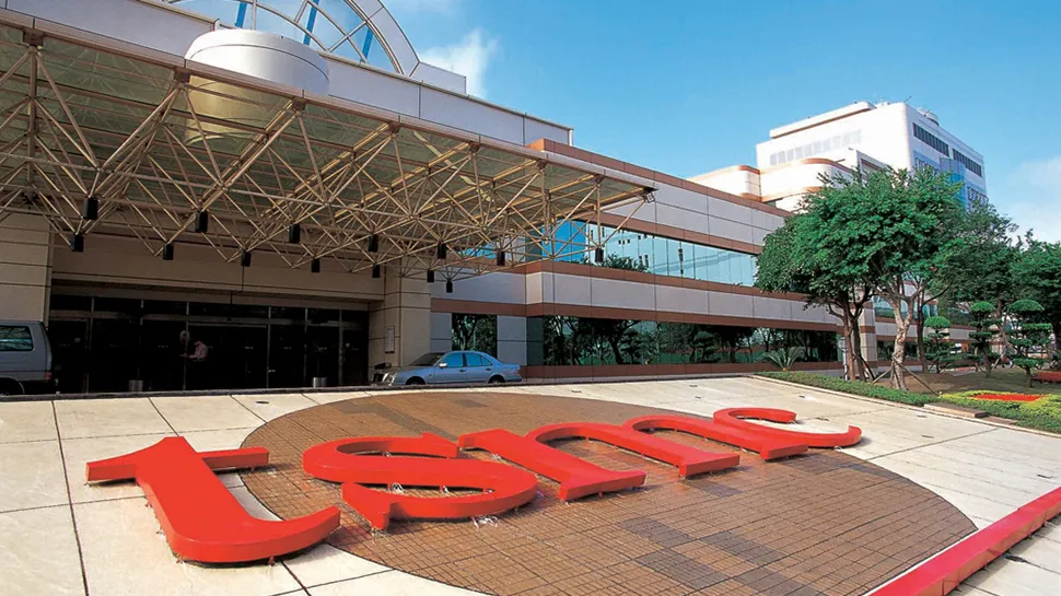
Taiwan Semiconductor Manufacturing Co. this week held a beam-raising ceremony for its new manufacturing facility at the Southern Taiwan Science Park near Tainan. The fab is expected to start volume production of chips using the company's N3 process technology in the second half 2022.
TSMC started to construct its new production facility in late October, 2019. The company will start moving in equipment in the coming months and the factory will be completed in 1 – 1.5 years from that moment. Mark Liu, TSMC's chairman, said at the ceremony that the facility would have a production capacity of around 55,000 300 mm wafer starts per month (WSPM) using the company's N3 fabrication process when it becomes fully operational in the second half of 2022.
The company was allowed to begin construction of the fab in 2018 and, back then, the cost of the factory was estimated at $19.5 billion. Traditionally, TSMC builds its factories in several phases, but at this time, the company did not disclose whether it had completed construction of buildings for all phases, or just the first one. Meanwhile, since TSMC usually builds the so-called 'gigafabs' (semiconductor manufacturing facilities with production capacity of over 100,000 WSPMs), it is likely that we are dealing with the first phase of a major project.
TSMC already operates Fab 14 and Fab 18 (which is yet to be fully built) production facilities in Southern Taiwan Science Park near Tainan, so the new fab will complement them. At present, TSMC employs about 15,000 people at Fab 14 and Fab 18. After the Fab 18 is fully built and the new facility becomes operational, the number of TSMC employees at the Tainan area will increase to around 20,000.
TSMC's N3 fabrication process will use FinFET transistor structures and is designed for both mobile and high-performance computing applications. The 3nm manufacturing technology promises to deliver an up to 15% performance gain (at the same power and transistor count), an up to 30% power reduction (at the same clocks and complexity), and an up to 70% logic density increase. The new node is said to use extreme ultraviolet lithography (EUVL) for up to 'over 20 layers,' something that no new processes do today.
Earlier this month it transpired that TSMC had placed a massive order for ASML's Twinscan NXE extreme ultraviolet (EUV) scanners that were expected to be used for one of its upcoming production facilities.
Source: DigiTimes, GizChina, TaiwanNews
