TSMC brings its most advanced chipmaking node to the US yet, to begin equipment installation for 3nm months ahead of schedule — Arizona fab slated for production in 2027
Much earlier than expected
TSMC is set to start moving equipment into its Fab 21 phase 2 in Arizona next summer, according to Nikkei, which cites sources familiar with the plan. Once the supporting and production tools are installed sometimes in 2027, the company will be able to start mass production of chips using its N3 technology, several quarters ahead of schedule.
TSMC will begin installation of equipment into its Fab 21 phase 2 in Arizona in the third calendar quarter — from July to September — of 2026, with the aim to start production at the facility in calendar 2027, several quarters ahead of the original schedule of 2028, if the report from Nikkei is accurate.
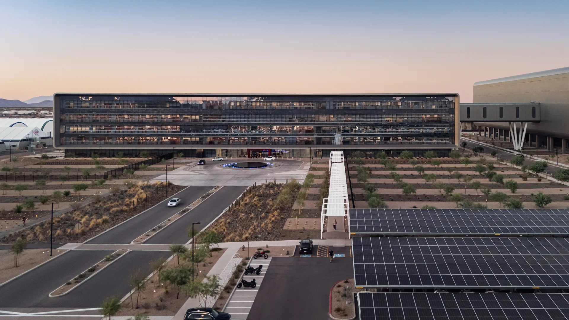
Construction of TSMC's Fab 21 phase 2 in Arizona was completed this year, according to the company. After the building itself, as well as its mechanical/electrical/plumbing systems, are complete, chipmakers begin to install internal infrastructure like elevators and HVACs. Once this phase is done, chip producers perform environmental qualification, and if everything — temperature, pressure, humidity — is stable, then actual production tools are moved in.
Depending on the tool, its installation and tuning take between hours and days, though high-end DUV and EUV lithography systems take significantly longer to install and tune than other machines at the fab. But in any case, it takes months to install the first group of tools, make them work in concert, and begin small-volume mass production. That said, TSMC has a chance to initiate mass production of chips on its N3 manufacturing technology in Arizona already in 2027, though volumes will be limited.
TSMC began to build its N2/A16-capable Fab 21 phase 3 in Arizona in April, 2025. The company hopes to complete this one as fast as possible to start output of its 2nm and 1.6nm-class chips in America ahead of schedule as well.
"With the strong collaboration and support from our leading U.S. customers and the U.S. federal, state, and city government, we continue to speed up our capacity expansion in Arizona," C.C. Wei, chief executive of TSMC, said at the most recent earnings call in October. "We are making tangible progress and executing well to our plan. In addition, we are preparing to upgrade our technologies faster to N2 and more advanced process technologies in Arizona, given the strong AI-related demand from our customers."
Follow Tom's Hardware on Google News, or add us as a preferred source, to get our latest news, analysis, & reviews in your feeds.
Get Tom's Hardware's best news and in-depth reviews, straight to your inbox.

Anton Shilov is a contributing writer at Tom’s Hardware. Over the past couple of decades, he has covered everything from CPUs and GPUs to supercomputers and from modern process technologies and latest fab tools to high-tech industry trends.
-
hotaru251 Reply
TSMC brings its most advanced chipmaking node to the US yet
why is there a "yet" that makes no sense?
Also its not the most advanced node (its legally not able to have their most advanced nodes outside of Taiwan and you did an article on it a yr ago https://www.tomshardware.com/tech-industry/tsmc-cannot-produce-2nm-chips-overseas-until-domestic-output-becomes-more-advanced-confirms-taiwanese-govt-official).
TSMC's own website shows their that 2nm is their most advanced atm. -
thestryker Reply
Yet as in at this time. It's their most advanced manufacturing process on US shores.hotaru251 said:why is there a "yet" that makes no sense?
Also its not the most advanced node (its legally not able to have their most advanced nodes outside of Taiwan and you did an article on it a yr ago https://www.tomshardware.com/tech-industry/tsmc-cannot-produce-2nm-chips-overseas-until-domestic-output-becomes-more-advanced-confirms-taiwanese-govt-official).
TSMC's own website shows their that 2nm is their most advanced atm.
While I'd prefer a less clunky title it is accurate (also I'd much prefer they used node names instead of node "class" given how little the measurements mean). -
hotaru251 Reply
yes however title and that are much differentthestryker said:It's their most advanced manufacturing process on US shores. -
thestryker Reply
You're still misunderstanding the wording.hotaru251 said:yes however title and that are much different
TSMC brings its most advanced chipmaking node to the US yet
The meaning of "yet" in this context is "at this time"/"so far". Meaning that this is the most advanced node they've brought to the US to date. -
timsSOFTWARE They're 3 million months ahead of schedule - sounds like an enviable position to be in.Reply
In seriousness though, it's because they have 2nm in the works in Taiwan that they are allowed to bring 3nm here - so I don't know if you can really call it their "most advanced" node. (And I actually do mean here - I live about 3 miles from the current TSMC fab in Phoenix).