GeForce2 Scaling Analysis
Get Tom's Hardware's best news and in-depth reviews, straight to your inbox.
You are now subscribed
Your newsletter sign-up was successful
The GeForce2 Family
| Row 0 - Cell 0 | GeForce2 MX | GeForce2 GTS | GeForce2 Pro | GeForce2 Ultra |
| Chip Clock | 175 MHz | 200 MHz | 200 MHz | 250 MHz |
| Memory Type | DDR or SDR SDRAM | DDR SDRAM | DDR SDRAM | DDR SDRAM |
| Memory Clock | 166 MHz | 2x 166 MHz DDR | 2x 200 MHz DDR | 2x 230 MHz DDR |
| Memory Size | 16, 32 MB | 32, 64 MB | 32, 64 MB | 32, 64 MB |
| Interface | AGP 4x | AGP 4x | AGP 4x | AGP 4x |
| TV Out | Optional | Optional | Optional | Optional |
| TwinView | Yes | No | No | No |
| Process | 0.18 | 0.18 | 0.18 | 0.18 |
| Pixel Fill-Rate | 350 MPixel/s | 800 MPixel/s | 800 MPixel/s | 1 GPixel/s |
| Texel Fill-Rate | 700 MTexel/s | 1.6 Gtexel/s | 1.6 Gtexel/s | 2 Gtexel/s |
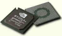
The GeForce2 MX is a slimmed derivate of the GeForce2 family. The GTS, Pro and Ultra models use exactly the same chip design, just running at different clock speeds.
The abandonment of features with the MX is not only cutting performance, but is also an advantage in terms of production costs and power consumption. Many MX cards do not require any active cooler.
Instead of 4 pixel pipelines, the MX does only have two. In addition the memory interface does not have to be 128-bit wide like with the other chips, but can optionally be 64-bit (even though hardly anybody builds this configuration). Last but not least, the chip clock has been reduced to 175 MHz.
Get Tom's Hardware's best news and in-depth reviews, straight to your inbox.
Current page: The GeForce2 Family
Prev Page Introduction Next Page Fast CPU Or High-End Graphics Card?
Patrick Schmid was the editor-in-chief for Tom's Hardware from 2005 to 2006. He wrote numerous articles on a wide range of hardware topics, including storage, CPUs, and system builds.
