BIOS And Overclocking
Swipe to scroll horizontally
| BIOS Frequency and Voltage settings (for overclocking) | |
|---|---|
| FSB Frequency | 100 - 700 MHz (1 MHz) |
| Clock Multiplier Adjustment | Yes |
| DRAM Frequency | FSB x 1.0, 1.2, 1.25, 1.33, 1.5, 1.6, 1.66, 2.0 |
| PCIe Clock | 90 - 150 MHz (1 MHz) |
| CPU Vcore | 0.50000- 1.6000 - 2.35 Volts (0.00625/0.05 Volts) |
| CPU FSB Voltage | 1.20 - 1.55 Volts (0.05 Volts) |
| Northbridge (MCH) | 1.25 - 2.025 Volts (0.15 Volts) |
| Southbridge (ICH) | None |
| DRAM Voltage | 1.50 - 3.05 Volts (0.05 Volts) |
| CAS Latency Range | |
| tCAS: 4-11; tRCD: 1-15; tRP: 1-15; tRAS: 1-63 |
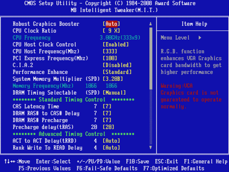
Though the X48T-DQ6 memory voltage range is different from that of the X48-DQ6, it appears the same since Gigabyte uses "over stock" settings rather than showing actual values. While the breadth of adjustments is identical, the base voltage for DDR3 is 1.50 volts rather than the 1.80 volts of DDR2.
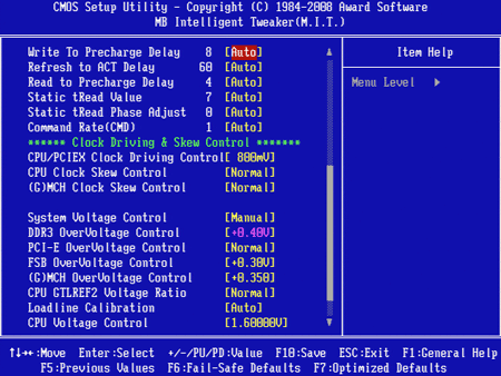
Our Core 2 Duo E6850 reached 4014 MHz clock at its stock 9x multiplier and 1.60 volts core. Dropping the CPU core multiplier to 6x allowed the X48T-DQ6 to reach 540 MHz FSB. FSB and MCH voltage were set to +0.30 V and +0.35 V respectively.
TOPICS
