Leaked photographs of an unidentified PCB (printed circuit board) originating from the Baidu forums are purportedly for AMD's upcoming 7nm Navi-based gaming graphics card.

There's no confirmation that the leaked PCB is indeed for the Navi graphics card, so take the information with a bit of salt. One thing is for sure though, the PCB design is fresh and doesn't seem like any of the PCBs that AMD has used in the past. Assuming that the PCB in question is Navi-based, it's likely an early engineering sample that's commonly used for internal testing only. The final product could still be subject to modifications.
| Row 0 - Cell 0 | AMD Navi | Radeon VII | RX Vega 64 | RX 590 | RX 580 | RTX 2080 Ti | RTX 2080 | RTX 2070 / RTX 2060 | GTX 1660 Ti / GTX 1660 | GTX 1650 |
| Architecture | Navi | GCN 5.1 | GCN 5.0 | GCN 4.0 | GCN 4.0 | Turing | Turing | Turing | Turing | Turing |
| GPU | ? | Vega 20 | Vega 10 | Polaris 30 | Polaris 20 | TU102 | TU104 | TU106 | TU116 | TU117 |
| Foundry | TSMC | TSMC | GloFlo | GloFlo | GloFlo | TSMC | TSMC | TSMC | TSMC | TSMC |
| Manufacturing Process | 7nm | 7nm | 14nm | 12nm | 14nm | 12nm | 12nm | 12nm | 12nm | 12nm |
| Transistor Count | ? | 13.2 billion | 12.5 billion | 5.7 billion | 5.7 billion | 18.6 billion | 13.6 billion | 10.8 billion | 6.6 billion | 4.7 billion |
| Die Size | 200 - 230 mm² | 331 mm² | 495 mm² | 232 mm² | 232 mm² | 754 mm² | 545 mm² | 445 mm² | 284 mm² | 200 mm² |
The mysterious PCB hosts a pretty small area for the Navi silicon. Current speculation is that the Navi die could measure anything from 200 to 230 mm², which doesn't sound too far-fetched considering that TSMC is reportedly producing Navi for AMD on the foundry's 7nm process node. If the die size is accurate, it will put Navi in the same ballpark as AMD's previous Polaris 20 silicon and Nvidia's present Turing TU117 silicon.
A recent report indicated that the future PlayStation 5 would sport a Navi graphics chip capable of ray tracing. Nvidia already offers real-time ray tracing support on its latest Turing-power graphics card. However, the Green Team's implementation involves baked-in RT cores into the Turing silicon that result in gargantuan dies, so Turing GPUs that lack the RT and Tensor cores are significantly smaller than the full-fledged Turing counterparts. It will be interesting to see how AMD implements ray tracing on Navi given its rumored die size.
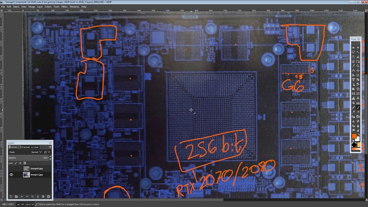
The alleged Navi die is surrounded by eight spaces reserved for memory chips. This means that the PCB could host an 8GB or 16GB configuration and probably sports a 256-bit memory interface, too. Buildzoid, a respected expert on motherboard and graphics card PCBs, noted that the memory spaces had room for a total of 180 pins (18x5x2), which coincides with the 180 ballout for GDDR6 chips. It's evident that Navi will employ GDDR6 memory.
| Header Cell - Column 0 | AMD Navi | Radeon VII | RX Vega 64 | RX Vega 56 | RTX 2080 Ti | RTX 2080 | RTX 2070 | RTX 2060 |
|---|---|---|---|---|---|---|---|---|
| Architecture (GPU) | Navi | Vega 20 | Vega 10 | Vega 10 | TU102 | TU104 | TU106 | TU106 |
| Shaders | ? | 3840 | 1408 | 3584 | 4352 | 2944 | 2304 | 1920 |
| Texture Units | ? | 240 | 256 | 224 | 272 | 184 | 144 | 120 |
| Base Clock Rate | ? | 1400 MHz | 1200 MHz | 1138 MHz | 1350 MHz | 1515 MHz | 1410 MHz | 1365 MHz |
| GPU Boost Rate | ? | 1750 MHz | 1536 MHz | 1474 MHz | 1545 MHz | 1710 MHz | 1620 MHz | 1680 MHz |
| Memory Capacity | 8GB or 16GB GDDR6 | 16GB HBM2 | 8GB HBM2 | 8GB HBM2 | 11GB GDDR6 | 8GB GDDR6 | 8GB GDDR6 | 6GB GDDR6 |
| Memory Clock | ? | 2 Gbps | 1.89 Gbps | 1.6 Gbps | 14 Gbps | 14 Gbps | 14 Gbps | 14 Gbps |
| Memory Bus | 256-bit | 4096-bit | 2048-bit | 2048-bit | 352-bit | 256-bit | 256-bit | 192-bit |
| Memory Bandwidth | ? | 1 TB/s | 483.8 GB/s | 409.6 GB/s | 616 GB/s | 448 GB/s | 448 GB/s | 336 GB/s |
| ROPs | ? | 64 | 64 | 64 | 88 | 64 | 64 | 48 |
| L2 Cache | ? | 4MB | 4MB | 4MB | 5.5MB | 4MB | 4MB | 3MB |
| TDP | 250W to 300W | 300W | 295W | 210W | 250W | 215W | 175W | 160W |
According to Buildzoid's observations, the PCB comes equipped with an eight-phase power delivery subsystem that features Smart Power Stage (SPS) modules. Past Radeon graphics cards used SPS packages rated for 70A, so we can expect the same for Navi. The PCB showcases spacing for two 8-pin PCIe power connectors. However, it's important to take into consideration that this is a test PCB after all, so don't go running for the pitchforks just yet. Based on the design of the power delivery subsystem and the power configurations, Buildzoid estimates that Navi's TDP (thermal design power) is somewhere between 250W to 300W. Power efficiency hasn't been AMD's strong suit so let's hope the company can prove us wrong.

The backside of the PCB doesn't reveal any noteworthy information. There's an array of pins that is presumably part of the LED indication system that dynamically changes the color of the LEDs to reflect the graphics card's load. Buildzoid also discovered a few configuration switches that may be exclusive to this engineering sample, or maybe they're for RGB lighting. No one knows at this point.
Lastly, the PCB and hole layout implies that this particular Navi graphics card will come with a reference blower design. Reference blowers don't always have the best reputation when it comes to cooling, but they work competently as long as the graphics card has a modest TDP. Display outputs include one HDMI port and two DisplayPort. It looks like AMD might be following in Nvidia's footsteps as there appears to be a USB-C port for virtual reality headsets.