Samsung 845DC EVO SSD Review: 3-Bit MLC Hits The Enterprise
With the introduction of its 845DC EVO, Samsung continues down the path of taking well-received enthusiast-oriented SSDs and customizing them for the enterprise. We run the new drive through a battery of tests in order to determine its strengths.
Inside Of Samsung's 845DC EVO
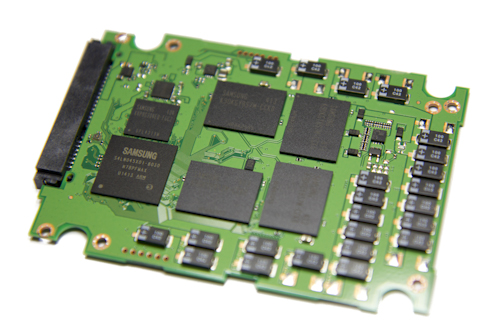
Opening up the 845DC EVO gives us flashbacks to our coverage of the 840 EVO. Its PCB and general layout, along with most of the components, are identical. Samsung's consumer-oriented 840 EVO employs a smaller PCB, which creates more empty space inside the 2.5" chassis. But the 845DC EVO's circuit board is larger to accommodate the power-loss protection capacitors, filling the enclosure.
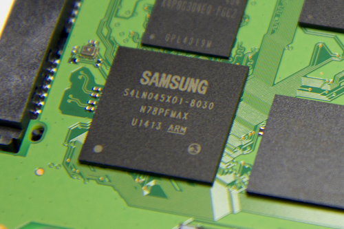
Samsung's 845DC EVO uses the same MEX 400 MHz triple-core Cortex-R4-based controller (labeled S4LN045X01-8030) as the 840 EVO.
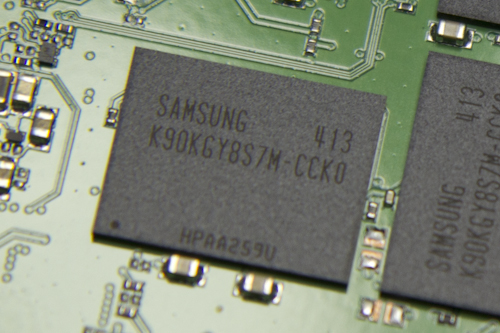
Also, the same 1 GB of LPDDR2 DRAM cache is present on the largest 845DC EVO model.
Article continues belowAs mentioned in the introduction, Samsung's 845DC EVO employs 3-bit-per-cell NAND. Our 960 GB review unit includes 1024 GiB of raw flash capacity. Each of the on-board packages contains eight dies, with 16 GiB per die. The spare area (12.7%) is greater than what the 840 EVO (9.05%) offers, helping improve consistency and extend the NAND's life.
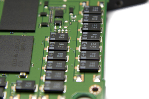
In the above shot, you can see some of the 23 power-loss capacitors used to keep the SSD's controller running just long enough, in the event of an outage, to flush all pending writes.
Overall, Samsung appears to take a direct approach to the 845DC EVO's design, only making changes deemed absolutely necessary. After all, the 840 EVO is already a fairly mature platform.
Get Tom's Hardware's best news and in-depth reviews, straight to your inbox.
Current page: Inside Of Samsung's 845DC EVO
Prev Page Meet Samsung's Read-Focused 845DC EVO SSD Next Page How We Test Samsung's 845DC EVO SSD-
SteelCity1981 So basicly it's the more durable version of the 840 evo much like opertons and xeons are to the FX and core i7 series.Reply -
Plusthinking Iq like we know now after the ssd endurance test samsung is the worst enterprise candidate.Reply -
drewriley Reply13419610 said:So basicly it's the more durable version of the 840 evo much like opertons and xeons are to the FX and core i7 series.
Yes, that's a fair analogy. Just like the Xeon E3-1275v3 is an i7-4770K, but with ECC support.
-
damric I've yet to see an SSD fail due to read/write endurance. I only see them fail when the controller gets bugged, which seems to happen all the time, especially on loss of power.Reply
-
soundping I'm guessing this SSD doesn't have to new firmware code that extends life and speed.Reply -
jase240 Another win for the EVO. This SSD modified for enterprise workloads makes it a good buy for webservers.Reply
Hopefully the price will go down after launch, and then I see this being the best choice of webhosts.
Cheaper and adequate for that workload. -
Nuckles_56 "Even still, I wand to commend Samsung's execution." (last page 1st paragraph) I guess that is supposed to be want, unless Drew Riley has become a wizard now :DReply -
drewriley Reply13426610 said:Commending their execution would be a bit harsh, don't you think?
I'm sure worse things were said about Samsung at WWDC '14 yesterday ;)


