AMD and Nvidia Platforms Do Battle
Nvidia GeForce 8200/8300 mGPU
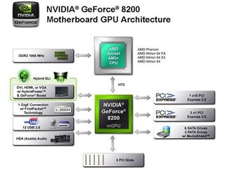
First of all, we need to address some confusion around the products GeForce 8200 and GeForce 8300, as there is no way to find out their differences on the Nvidia website. The GeForce 8300 probably was a reaction to AMD’s graphics performance with the 780G chipset, as the 8200 and 8300 are identical except for the clock speed of their 16 stream processors: the GeForce 8200 runs at 1.2 GHz, while the GeForce 8300 is clocked at a 1.5 GHz speed, providing improved 3D graphics performance.
Nvidia decided to emphasize the GeForce part of this integrated chipset, by dropping the nForce name. That’s also why Nvidia refers to it as the GeForce 8200/8300 mGPU – this stands for Motherboard GPU. The model number indicates a perfect fit into the GeForce 8 family, signifying that GeForce 8200 is actually the entry-level part.

Big Chip Beats Two-Way AMD Design
Unlike the AMD 780G chipset, the GeForce 8200/8300 mGPU is a single-chip solution, which isn’t even built on a top-notch manufacturing process. Nvidia utilizes an 80 nm process, which is good enough to hold all the chipset features, PCI Express 2.0 connectivity, SATA controller with legacy UltraATA, 12 USB 2.0 ports and a Gigabit Ethernet controller. Even with all that, the solution is still slightly more efficient than the 780G, requiring a system idle power of 58 W versus AMD’s 60 W using a Phenom X4 9600 processor.
Stay on the Cutting Edge
Join the experts who read Tom's Hardware for the inside track on enthusiast PC tech news — and have for over 25 years. We'll send breaking news and in-depth reviews of CPUs, GPUs, AI, maker hardware and more straight to your inbox.
Current page: Nvidia GeForce 8200/8300 mGPU
Prev Page ASRock A780FullDisplayPort Utilities Next Page GeForce 8200 Graphics with PureVideo HDMost Popular

