IBM Makes World's Smallest 3D Map with Nanotech
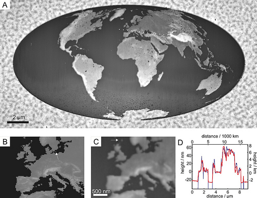
Scientists from IBM have created a 3D map of the world that is so small, 1,000 of them could fit on a single grain of salt.
IBM this week reports that by using a new much less complex technique that involves a tiny, silicon tip (100,000 times smaller than the tip on a sharpened pencil), scientists can create patterns as small as 15 nanometers for much less money.
"Advances in nanotechnology are intimately linked to the existence of high-quality methods and tools for producing nanoscale patterns and objects on surfaces," explains physicist Dr. Armin Knoll of IBM Research – Zurich. "With its broad functionality and unique 3D patterning capability, this nanotip-based patterning methodology is a powerful tool for generating very small structures."
IBM says that this patterning technique opens new prospects for developing nano-sized objects in fields such as electronics, future chip technology, medicine, life sciences, and optoelectronics. However, for now, they're having fun making teeny, tiny 3D maps of the world.
Check out the video below to see how the technology works.
Get Tom's Hardware's best news and in-depth reviews, straight to your inbox.

Jane McEntegart is a writer, editor, and marketing communications professional with 17 years of experience in the technology industry. She has written about a wide range of technology topics, including smartphones, tablets, and game consoles. Her articles have been published in Tom's Guide, Tom's Hardware, MobileSyrup, and Edge Up.
-
micr0be next step is adding color ...... black and white 3d nanometer scale of the world is so 10 years agoReply -
eklipz330 omg imagine the number of formulas i can right on my thumbnail for finals with this...Reply -
tommysch eklipz330omg imagine the number of formulas i can right on my thumbnail for finals with this...Reply
But the 10 foot tall microscope that you'll need to read them might give you away. -
micr0be TommySchBut the 10 foot tall microscope that you'll need to read them might give you away.Reply
also he spelled "right" wrong, so i think they'll just pretend they can't see anything anyway, and let him cheat.
-
eklipz330omg imagine the number of formulas i can right on my thumbnail for finals with this...Never mind your thumbnail, use a contact lens instead. :DReply
But then again, everyone in the class would be wondering why you look so cross eyed during the test! -
longshotthe1st Renegade_WarriorNever mind your thumbnail, use a contact lens instead. But then again, everyone in the class would be wondering why you look so cross eyed during the test!Reply
They should be looking at their own papers, not him!! lol -
darkknight22 Minus_i7Clearly what the eco-terrorists were trying to stop.Reply
exactly, because this is going to DESTROY the environment -
Doctor-boom For all we know the map could be purple with yellow dots: it's viewed using a scanning electron microscope, which does not see colors, at ALL. You can color code the image differently than black and white, but it really look nicer this way. Note that you are not "seeing" the object really: a detector is telling the machine how many electrons came from that point on your sample, so it does not always work in the same way as a light generated image.Reply
