Intel Core i7 (Nehalem): Architecture By AMD?
Get Tom's Hardware's best news and in-depth reviews, straight to your inbox.
You are now subscribed
Your newsletter sign-up was successful
QuickPath Interconnect
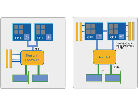
While the Core architecture was remarkably efficient, certain design details had begun to show their age, first among them the Front Side Bus (FSB) system. This bus connecting the processors to the northbridge was a real anachronism in an otherwise highly modern architecture. The major fault was most noticeable in multiprocessor configurations, where the architecture had a hard time keeping up with increasing loads. The processors had to share this bus not only for access to memory, but also for ensuring the coherence of the data contained in their respective cache memories.
In this kind of situation, the influx of transactions to the bus can lead to its saturation. For a long time, Intel simply worked around the problem by using a faster bus or larger cache memories, but it was high time for them to address the underlying cause by completely overhauling the way its processors communicate with memory and outside components.
The solution Intel chose—called QuickPath Interconnect (QPI)—was nothing new; an integrated memory controller is an extremely fast point-to-point serial bus. The technology was introduced five years ago in AMD processors, but in reality it’s even older than that. These concepts, showing up in AMD and now Intel products, are in fact the result of work done ten years ago by the engineers at DEC during the design of the Alpha 21364 (EV7). Since many former DEC engineers ended up in Santa Clara, it’s not surprising to see these concepts surfacing in the latest Intel architecture.
From a technical point of view, a QPI link is bidirectional and has two 20-bit links—one in each direction—of which 16 are reserved for data; the four others are used for error detection codes or protocol functions. This works out to a maximum of 6.4 GT/s (billion transfers per second), or a usable bandwidth of 12.8 GB/s, both read and write. Just for comparison, the FSB on the most recent Intel processors operates at a maximum clock frequency of 400 MHz, and address transfers need two clock cycles (200 MT/s) whereas data transfers operate in QDR mode, with a bandwidth of 1.6 GT/s. With its 64-bit width, the FSB also has a total bandwidth of 12.8 GB/s, but it’s usable for writing or reading.
So a QPI link has a theoretical bandwidth that’s up to twice as high, provided reads and writes are well balanced. In a theoretical case consisting of reads only or writes only, the bandwidth would be identical to that of the FSB. However, you have to keep in mind that the FSB was used both for memory access and for all transfers of data to peripherals or between processors. With Nehalem, a QPI link will be exclusively dedicated to transfers of data to peripherals, with memory transfers handled by the integrated controller and inter-CPU communications in multi-socket configurations by another QPI link. Even in the worst cases, a QPI link should show significantly better performance than the FSB.

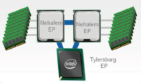
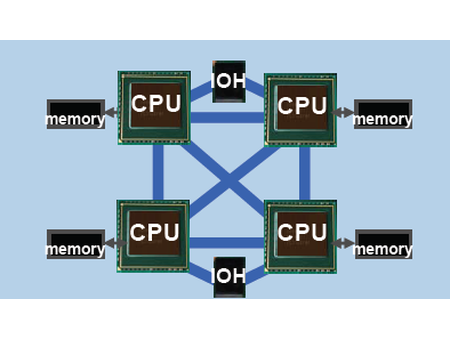
As we’ve seen, Nehalem was designed to be a flexible, scalable architecture, and so the number of QPI links available will vary with the market segment being aimed at—from one link to the chipset for single-socket configurations to as many as four in four-socket server configurations. This enables true fully-connected four-processor systems, meaning that each processor can access any position in memory with a maximum of a single QPI link hop since each CPU is connected directly to the three others.
Get Tom's Hardware's best news and in-depth reviews, straight to your inbox.
Current page: QuickPath Interconnect
Prev Page SSE 4.2 And Power Consumption Next Page Memory Subsystem-
cl_spdhax1 good write-up, cant wait for the new architecture , plus the "older" chips are going to become cheaper/affordable. big plus.Reply -
neiroatopelcc No explaination as to why you can't use performance modules with higher voltage though.Reply -
neiroatopelcc AuDioFreaK39TomsHardware is just now getting around to posting this?Not to mention it being almost a direct copy/paste from other articles I've seen written about Nehalem architecture.I regard being late as a quality seal really. No point being first, if your info is only as credible as stuff on inquirer. Better be last, but be sure what you write is correct.Reply
-
cangelini AuDioFreaK39TomsHardware is just now getting around to posting this?Not to mention it being almost a direct copy/paste from other articles I've seen written about Nehalem architecture.Reply
Perhaps, if you count being translated from French. -
randomizer Yea, 13 pages is quite alot to translate. You could always use google translation if you want it done fast :kaola:Reply -
Duncan NZ Speaking of french... That link on page 3 goes to a French article that I found fascinating... Would be even better if there was an English version though, cause then I could actually read it. Any chance of that?Reply
Nice article, good depth, well written -
neiroatopelcc randomizerYea, 13 pages is quite alot to translate. You could always use google translation if you want it done fast I don't know french, so no idea if it actually works. But I've tried from english to germany and danish, and viseversa. Also tried from danish to german, and the result is always the same - it's incomplete, and anything that is slighty technical in nature won't be translated properly. In short - want it done right, do it yourself.Reply -
neiroatopelcc I don't think cangelini meant to say, that no other english articles on the subject exist.Reply
You claimed the article on toms was a copy paste from another article. He merely stated that the article here was based on a french version. -
enewmen Good article.Reply
I actually read the whole thing.
I just don't get TLP when RAM is cheap and the Nehalem/Vista can address 128gigs. Anyway, things have changed a lot since running Win NT with 16megs RAM and constant memory swapping. -
cangelini I can't speak for the author, but I imagine neiro's guess is fairly accurate. Written in French, translated to English, and then edited--I'm fairly confident they're different stories ;)Reply


