Tom's Hardware Visits STMicroelectronics In Rennes, France
Operations At The Site
Two major factors account for the growth of STMicroelectronics’ Rennes site over past 10 years.
Marketing Advantages
The aerospace market is growing by approximately five percent per year, and the company has taken advantage of the trend. Its chips equip the Curiosity Mars rover, but also Galileo, the European GPS system, Meteosat, the Ariane launcher, the Astra television broadcasting satellites, the SPOT Earth observation satellite, and almost all satellites launched today.

Its customers include equipment manufacturers who sell parts of satellites, but also satellite manufacturers themselves. Its biggest client is the European Space Agency and its alter ego in France, the CNES (Centre National d’Études Spatiales), since STMicroelectronics gives it independence from the U.S. That takes concrete form in financing for development projects. The company also works with private players around the world and has privileged relationships with the European satellite systems integrators Thales-Alenia and EADS-Astrium.
Technological Advantages
The other factor that explains STMicroelectronics’ growth in this market and the explosion of activity at Rennes lies in the technologies the site can produce. Satellite manufacturers are not looking for the latest SoCs or the highest frequencies. They want mature technologies that have been proven over several years. For a satellite that will spend 20 years in orbit, reliability is much more important than using the latest fabrication process.
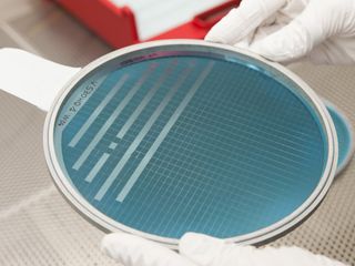
Concretely, the chips sold by STMicroelectronics use processes that date back three to five years (the company is currently working on qualification of 65 nm chips), but it also markets wafers that use a 7.5 µm (7,500 nm) process. That’s an advantage, because it has the only fab in the world that can still use that process, which dates from the 1970s, yet is still quite appropriate for high-reliability applications. One of the best-selling transistors for aerospace use is the 2N2222, introduced by Motorola in 1962.

Obviously, its production has been adapted to the new standards that govern fabrication, and the maturity of the technologies has resulted in optimized fabrication methods. Still, STMicroelectronics’ strength lies in the fact that it’s one of the rare companies in the world that can produce older-generation chips and make a profit.
Finally, there’s also a technological advantage in being able to take the time necessary to develop chips for aerospace use. Unlike certain components for consumer devices that take six months between development and marketing, four and five years can go by between the time a chip is developed and the time it’s marketed. Being able to maintain the necessary investments during that period requires resources that aren’t available to all chip makers on the market.
Current page: Operations At The Site
Prev Page Highly Rigorous Tests Next Page Challenges For The Rennes SiteStay on the Cutting Edge
Join the experts who read Tom's Hardware for the inside track on enthusiast PC tech news — and have for over 25 years. We'll send breaking news and in-depth reviews of CPUs, GPUs, AI, maker hardware and more straight to your inbox.
-
Scionyde "The poor overall economic picture and pessimistic approach newspapers like to take in speaking of the electronics industry in France would lead you to think that that scenario is utopian at best."Reply
Maybe I'm missing something obvious, but isn't 'utopian' the exact opposite of the word you were intending to use there? -
vancedecker This is really cool. A totally unexpected article in the swamp of cell phone reviews and press releases, on other sites...Reply -
army_ant7 @ScionydeReply
I'm thinking that "utopian" was used in a way to mean something highly unachievable, unlikely, or unfeasible. I'm not sure how that would apply though and I can't speak for the author. I'm not sure if this helps explain that... -
vaughn2k "Once the die is mounted in its case, the wires must be soldered to connect the chip and the pins. This operation can seem archaic compared with the processors used in PCs or smartphones, whose dies are connected via direct contact with bumps on their epoxy carriers." - The wire is not soldered to the pins but welded using an ultrasonic force + power - or Ultrasonic wirebonding. The head of the tool where the wire (either it is an Al or Au wire) comes out, generates this combination of ulrasonic energy to be able to connect the die pad and pins. If an Au wire is used, the process adds a thermal property, which is also called thermosonic bonding. CPU and smart phone chips (and virtually all chips) uses the same process. However, most assembly uses Au wire or Cu wire, instead of Al wire. Another process that is used o intorconnect chips to substrate is called flip-chip bonding, or soldering or ILB (inner lead bonding), and then going into the process of underfilling, to protect these interconnects.Reply -
vaughn2k "The testing also checks for the presence of particles inside the packages" - It is called PIND test (Particle Impact Noise Detection). It is in MIL-STD 883E method 2020.8 -- ;)Reply -
WyomingKnott What double-post? I don't see one.Reply
More practically, you should be able to delete your own post by going to the forum version of the comments. Click on the blue icon with quotation marks, full-edit the duplicate post, and there should be a delete button. -
Hey, and what about Goodram? Isn't it the last european based manufacturer of ram, flash, ssd etc? Can you please make a small trip there as well?Reply
