All three leading-edge foundries — Intel Foundry, Samsung Foundry, and TSMC — have initiated mass production of chips using 2nm-class process technology. Samsung was the first one to start production using its SF2 node (though it could be argued that this is a rebadged SF3P) around mid-2025, Intel followed suit with its 18A node in November (albeit at development lines in Oregon, not production lines in Arizona), and TSMC initiated high-volume manufacturing using its N2 process at two volume fabs in Taiwan in December. We outline what's next for these three leading-edge foundries.
The current state of the market
The amount of capital, expertise, and experience required to develop leading-edge process technologies and build high-volume fabs supporting advanced nodes is so high that only three companies in the world are currently capable of producing them. Companies like Rapidus have yet to prove they are a viable leading-edge chipmaker. Meanwhile, all three leading foundries are transitioning from traditional node scaling to a more segmented, architecture- and product-driven approach, but are doing so with different priorities.
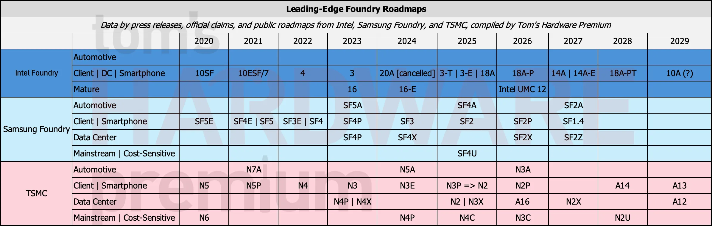
(Image credit: Tom's Hardware)
TSMC is focused on predictable scaling, combined with aggressive specialization, which is why its roadmap is split into high-performance computing-oriented technologies with backside power delivery network (BSPDN) and cost/density-optimized nodes without it.
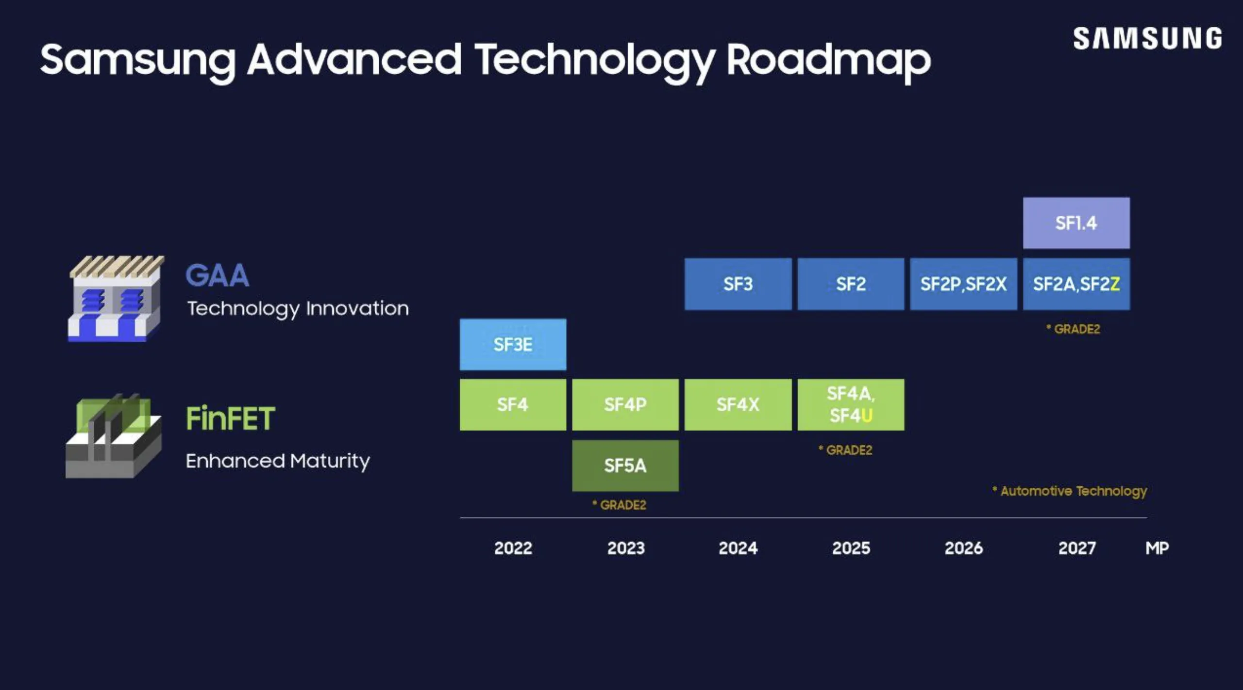
Samsung has a wide range of node variants, though it is currently more focused on yield improvement, rather than on scaling, which is why its roadmap appears more iterative than breakthrough-focused. This is perhaps why it is behind competitors with its BSPDN implementation.
Intel seems to be pursuing the most aggressive technological roadmap with a conjoined implementation of gate-all-around (GAA) RibbonFET transistors and PowerVia BSPDN, rapid iteration, and the aggressive pursuit of High-NA EUV lithography in 2027 – 2028, years before its rivals.
Intel Foundry: The most ambitious chipmaker
Being a new player in the foundry market and a large integrated design manufacturer (IDM), Intel is pursuing a multi-faceted strategy aimed at addressing the needs of its own products, as well as attempting to land customers that do not necessarily require leading-edge process technologies.
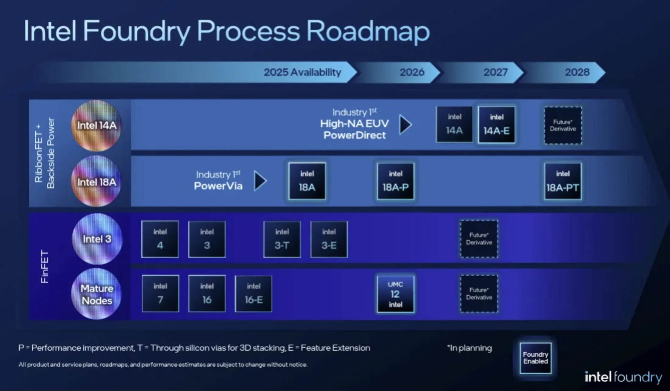
(Image credit: Intel/Tom's Hardware)
Intel's roadmap is the most ambitious, but arguably the most volatile one, when compared to the plans of other leading foundries. On the one hand, Intel needs the best fabrication technologies to differentiate its own consumer and data center products. To that end, with its 18A and subsequent process technologies, Intel bet on the simultaneous implementation of GAA transistors and a BSPDN to maximize performance, power efficiency, and transistor density. On the other hand, since Intel has zero customers from the automotive and smartphone sectors, it does not have any technologies tailored specifically for these applications.
Swipe to scroll horizontally
Row 0 - Cell 0
18A vs 3
18A vs 20A
18A-P vs 18A
14A vs 18A
14A-E vs 14A
Power
15% perf. per watt
10% perf. per watt
18%
25% - 35%
lower
Performance
15% perf. per watt
10% perf. per watt
9%
15% - 20%
higher
Density*
1.3X
slightly higher
-
1.3X
higher
Transistor
RibbonFET GAA
RibbonFET GAA
RibbonFET GAA
2nd Gen RibbonFET GAA
2nd Gen RibbonFET GAA
Power Delivery
PowerVia BSPDN
PowerVia BSPDN
PowerVia BSPDN
PowerDirect BSPDN
PowerDirect BSPDN
High Volume Manufacturing
H2 2025
H2 2025
2027 (?)
2028 (?)
2029 (?)
Intel's 18A is probably the most important technology for the company in years, as it will return production of the company's consumer CPUs back to its own fabs, something that promises to greatly improve margins. Although the company is in the process of improving yields on 18A and current 18A volumes are not significant, Intel is already preparing follow-on refinements such as 18A-P (with enhanced performance and improved power efficiency) and 18A-PT (which supports through silicon vias (TSVs) and can be used for 3D-integrated systems-in-package).
Beyond that, Intel is targeting 14A and 14A-E for 2027 ~ 2028 production readiness and an early ramp. The nodes will introduce Intel's 2nd Generation RibbonFET GAA transistors, revamped PowerDirect backside power delivery, and Turbo Cells to improve the performance of critical data paths.
These will be the company's first nodes to use High-NA EUV lithography, at least for some 14A and 14A-E variants, which will be another attempt to introduce a technology that will differentiate Intel compared to competing nodes. Intel has said that the interest in 14A from external customers is significant. Musk's Terafab project is set to make use of Intel's 14A, as a licensee, but not as a customer.
At the same time, Intel is heavily relying on node variants to address different use cases, including performance enhancements (P), feature enhancements (E), and through-silicon via support (T). These process technologies are required to enable Intel to build custom multi-chiplet products for consumer and data center applications, which directly support its strategy to produce most of its products at in-house fabs.
Intel's roadmap also includes continued investment in mature nodes such as Intel 16 and UMC 12 as the company pursues a strategy to capture demand outside leading-edge applications, to ensure steady revenue streams.
While Intel's plans are aggressive and ambitious, the abrupt cancellation of 20A in late 2024 highlights the execution risks associated with such a roadmap.
Samsung Foundry: When yields matter more than nodes
Samsung was the first company to adopt GAA transistors with its SF3E technology in 2022, three years before Intel and TSMC. However, low and unpredictable yields have limited the adoption of this technology to niche applications like cryptocurrency mining ASICs. While SF3 was more mature, it was still adopted by select applications, mostly internally. As a result, the highest-performing chips made by Samsung are produced using FinFET-based SF4P and SF4X, which puts the company behind its rivals.
(Image credit: Samsung)
For now, reducing defect density, increasing yields, and ensuring stable yields are the top priorities for Samsung. Last year, it began making mobile system-on-chips (SoCs) using its SF2 node (which it calls the 1st Generation 2nm GAA process), but among the major goals for the company for this year is to ramp up '2nd Generation 2nm [SF2P] and prepare performance and power-optimized 4nm process,' which suggests limited adoption of SF2. The fact that the low-power 4nm-class node will be a major workhorse for the company. The company's roadmap also indicates SF2X (HPC-oriented) in 2026 as well as SF2A (for automotive applications) and SF2Z (SF2X with BSPDN) in 2027, though we can only wonder whether these nodes will be widely adopted.
Nonetheless, Samsung's iterative approach to the evolution of its SF2 nodes (SF2=>SF2P=>SF2X=>SF2X with backside power) is evident, which gives us hope that the company's yields will gradually improve.
Samsung's next major node will be SF1.4, a 1.4nm-class process technology optimized for consumer and smartphone applications, which won't feature backside power delivery. Samsung's slides put SF1.4 above the SF3 and SF2 families, which may suggest that this manufacturing process will feature some major enhancements, such as a new GAA transistor design or other major refinements. Samsung expects to mass-produce chips on its SF1.4 technology in 2027, so it can formally leave Intel and TSMC behind with its 1.4nm node.
A big question lingers, and that's whether Samsung plans to finally start using pellicles with its EUV lithography tools starting with SF1.4, or later. A lack of pellicles greatly increases the number of potentially yield-killing stochastic mask-borne defects, which are increasingly dominant at the 2nm and are getting much worse at thinner nodes.
TSMC: New technologies like clockwork
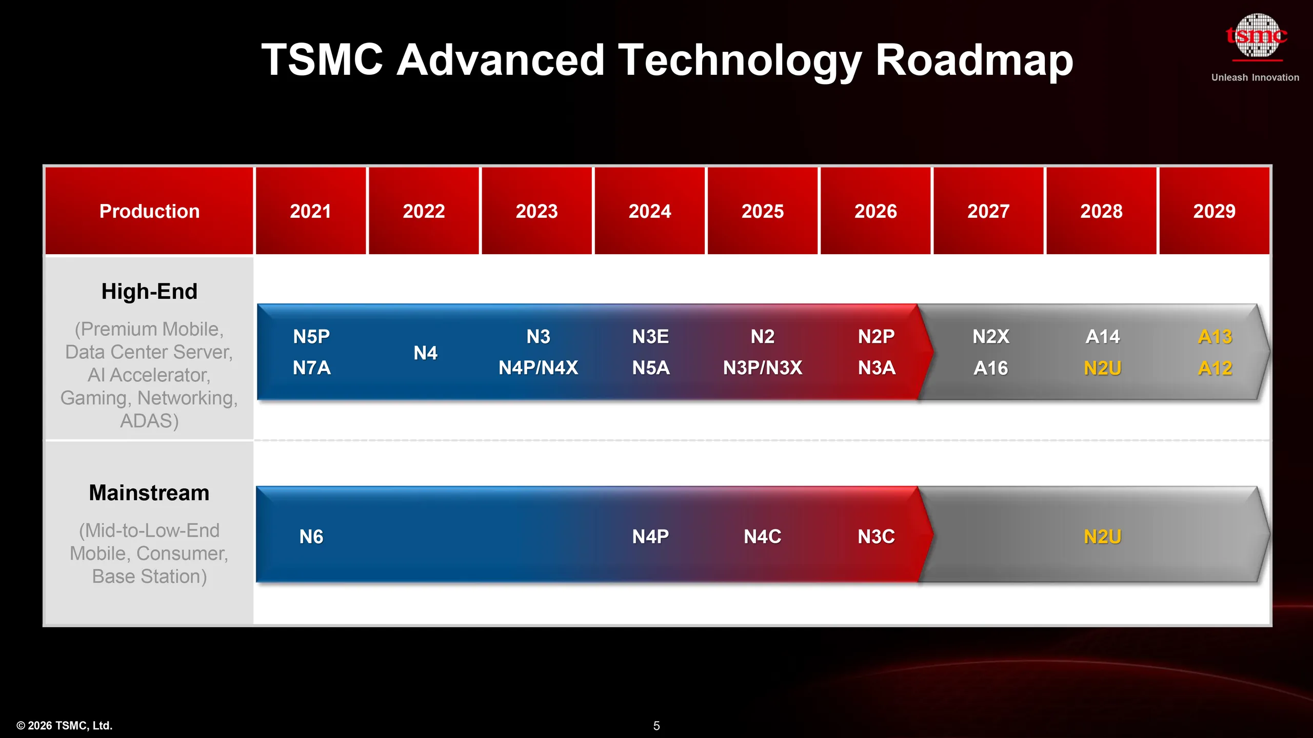
TSMC's roadmap remains the most structured and execution-focused among the three. The world's largest contract chipmaker initiated mass production of chips using its N2 process technology — its first node with GAA nanosheet transistors — at two fabs simultaneously late last year in a bid to meet demand from a wide range of applications, starting from Apple's smartphones and all the way to AMD's server-bound EPYC 'Venice' CPUs. Initiating volume production at two fabs simultaneously is something that rarely happens in the industry, though it looks like structural changes caused by demand from the AI segment are changing many things in the industry.
Swipe to scroll horizontally
Row 0 - Cell 0
A16 vs N2P
N2X vs N2P
N2U vs N2P
A14 vs N2
A13 vs A14
A12 vs A16
Power
-15% ~ -20%
lower
8% - 10%
-25% ~ -30%
?
lower
Performance
8% - 10%
10%
3% - 4%
10% - 15%
?
higher
Chip Density*
1.07x - 1.10x
?
?
1.2x
?
denser
Logic Density
?
?
1.02X - 1.03X
1.23x
1.06X
denser
Transistor
GAA
GAA
GAA
2nd Gen GAA
2nd Gen GAA
2nd Gen GAA
Power Delivery
SPR
Front-side w/ SHPMIM (?)
Front-side w/ SHPMIM (?)
Front-side w/ SHPMIM (?)
Front-side w/ SHPMIM (?)
SPR
High Volume Manufacturing
2027
2027
2027
2028
2029
2029
(Image credit: TSMC)
TSMC is on track to start making chips using performance-enhanced N2P with traditional frontside power delivery and A16 technology that adds backside power delivery on top, a split which highlights TSMC's increasingly segment-specific approach to leading-edge technologies.
Going forward, the company is set to continue offering advanced technologies with and without BSPDN, as this feature may be too expensive for consumer and smartphone applications, but is clearly valuable for heavy-duty data center processors. For example, A14 will emerge as a smartphone-oriented node in 2028, but then will re-emerge as a data center-oriented node once it gets BSPDN in 2029.
In addition, the company will continue to offer mainstream nodes like N4C, N3C, and eventually N2C for applications that are more sensitive to costs. Automotive-specific nodes (N7A, N5A, N3A) will lag leading-edge nodes by one to two generations, as they prioritize reliability and longevity over performance and transistor density.
TSMC's segmentation and yearly cadence for advanced manufacturing nodes enable the foundry to address the most demanding clients like Apple, AMD, Intel, Nvidia, or Qualcomm with competitive process technologies. Ultimately, such cadence and a wide range of nodes reinforce TSMC's position as the most predictable and commercially disciplined foundry.
Fractured futures
To sum things up, TSMC continues to bet on execution discipline and segmentation as it ramps its 2nm-class node at two fabs to meet overwhelming demand from a variety of applications, starting from humble cell phones all the way to heavy-duty servers.
Intel leads in architectural ambitions, as currently it is the only company that uses a process technology that features both gate-all-around transistors and backside power delivery. However, the company admits that its yields will only get to world-class level by 2027, which likely makes Intel's 18A node significantly less attractive to demanding customers.
Samsung sits somewhere in the middle, offering a wide variety of process technologies for different applications, but the company's yields with GAA-based nodes have been a challenge, which is why the firm is now focused on yield increases rather than on breakthroughs, so it does not attempt to leapfrog its competitors.
Anton Shilov is a contributing writer at Tom’s Hardware. Over the past couple of decades, he has covered everything from CPUs and GPUs to supercomputers and from modern process technologies and latest fab tools to high-tech industry trends.