Intel Plows $4.1 billion Into Next-Gen Chip Production
Intel is getting serious about 450 nm wafers and EUV, again.
Get Tom's Hardware's best news and in-depth reviews, straight to your inbox.
You are now subscribed
Your newsletter sign-up was successful
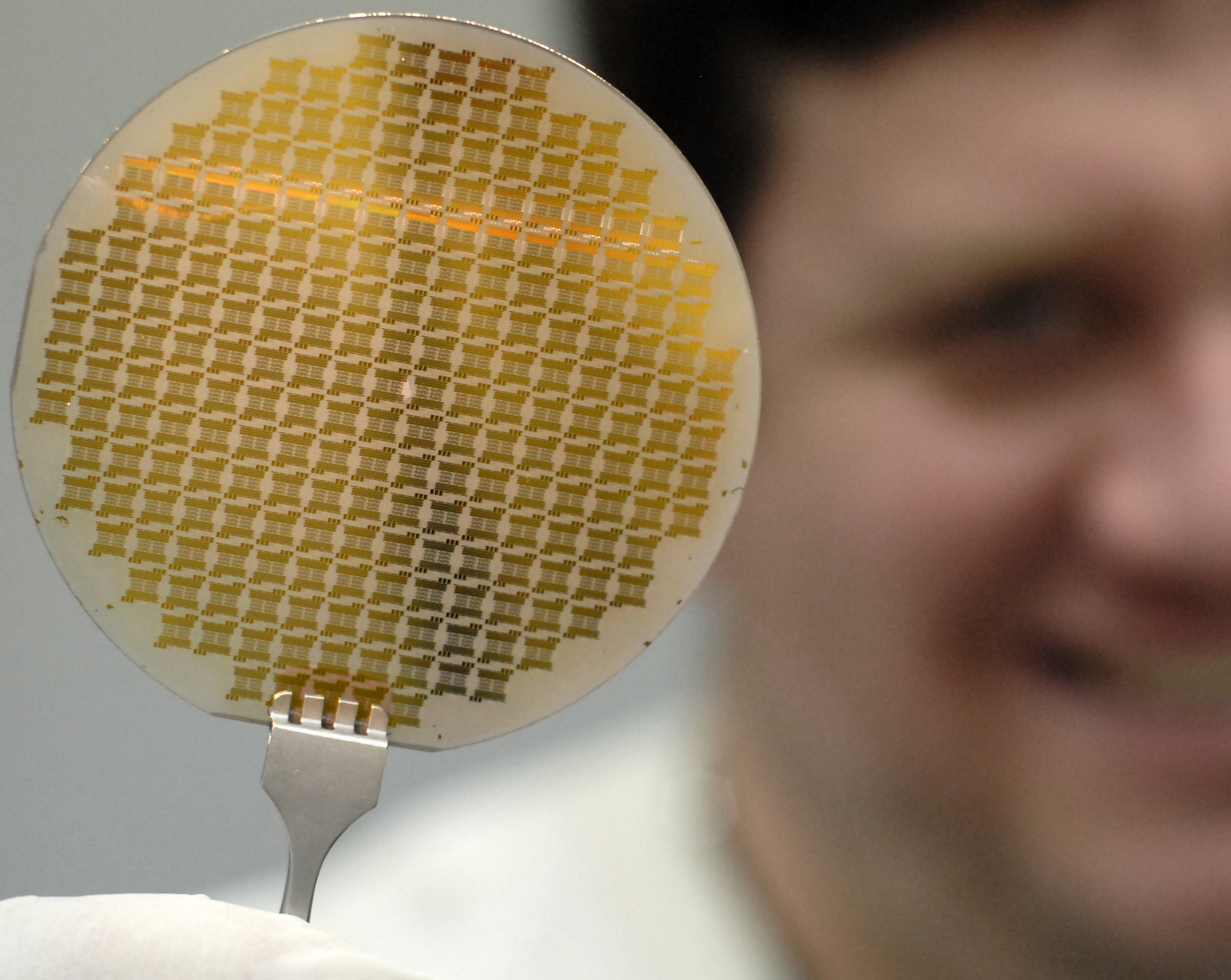
In a rather subtle announcement, Intel said that it has invested about $4.1 billion in ASML to accelerate the development of chip production on 450 nm wafers and extreme ultra-violet (EUV) lithography. The company transitioned from 200 mm to 300 mm wafers with its 130 nm chip generation, which was launched in 2001 with the Tualatin- and Coppermine-based Pentium III processors.
In about the same time frame, the company heavily discussed the transition of the production process to costly EUV, but found ways to extend conventional lithography methods, delay the massive EUV investment - about $125 million per production tool - that was originally planned to debut with 65 nm or 45 nm processors. By 2003, Intel had dropped EUV from its roadmap.
The ASML investment is the first major sign that EUV is resurfacing. The R&D investment in ASML is about $1.0 billion: Over a period of five years, $680 million will be spent on 450 mm development and about $340 million on EUV. The remaining $3.0 billion is an equity investment that grant Intel 15 percent share in ASML. The investment makes sense, as it allows Intel to drive production innovation and keep an edge in chip production technology, which is the company's most critical asset today.
Article continues belowIntel did not disclose additional 450 mm and EUV plans.
Get Tom's Hardware's best news and in-depth reviews, straight to your inbox.

Douglas Perry was a freelance writer for Tom's Hardware covering semiconductors, storage technology, quantum computing, and processor power delivery. He has authored several books and is currently an editor for The Oregonian/OregonLive.
-
CaedenV I loved my Coppermine CPU, it was the first build I ever did on my own, and beat most pentium 4 CPUs for the next 2 years on the benchmarks (due to RAMBUS more than the inherent flaws that later choked the P4 line). It was truly the last good CPU to come out of Intel until the Core series.Reply -
dragonsqrrl "Intel is getting serious about 450 nm wafers and EUV, again."Reply
Doug, I think you mean 450 mm, right? -
back_by_demand dragonsqrrl"Intel is getting serious about 450 nm wafers and EUV, again."Doug, I think you mean 450 mm, right?Either that or they are investing in 30 year old chip techReply -
captaincharisma i guess that whole time being 2nd to AMD gave intel that killer instinct. unfortunetly for AMD they do not turn it offReply -
tului back_by_demandEither that or they are investing in 30 year old chip techThe day they can get more than a few transistors out of 450nm of wafer, let me know. I'm almost positive he meant mm.Reply -
jimmysmitty captaincharismai guess that whole time being 2nd to AMD gave intel that killer instinct. unfortunetly for AMD they do not turn it offReply
Intel has always had better process manufaturing than anyone else, even AMD. Just not the best architecture. -
A Bad Day jimmysmittyIntel has always had better process manufaturing than anyone else, even AMD. Just not the best architecture.Reply
Well, currently Intel can absorb losses and drown its R&D department with cash. It's a good thing for AMD that Intel's GPU team didn't have as much success as the CPU team. -
thecolorblue A Bad DayIt's a good thing for AMD that Intel's GPU team didn't have as much success as the CPU team.true, yet Intel has finally started getting real serious about integrated graphics. AMD needs to turn on the juice, it would be nice to see Intel facing a more serious competitor from a consumer's wallet perspectiveReply -
zanny thecolorbluetrue, yet Intel has finally started getting real serious about integrated graphics. AMD needs to turn on the juice, it would be nice to see Intel facing a more serious competitor from a consumer's wallet perspectiveReply
For laptops Trinity chips are amazing. Intel is grossly overselling the entire Ivy Bridge mobile line and Trinity wipes the floor with them at a price to performance analysis. The integrated graphics being as good as they are only helps future proof them as more software takes advantage of SIMD processing. -
darkavenger123 This news like a final sword in the coffin for AMD. Make sure they'll never get up...NEVER,Reply
